Gallium arsenide-based Schottky frequency-doubling diode with multi-beam leads

A gallium arsenide-based, beam-lead technology, applied in the direction of semiconductor/solid-state device parts, semiconductor devices, electrical components, etc., can solve the problems of increasing scientific research costs, devices cannot be installed normally, and devices are scrapped, etc., to reduce Production and scientific research costs, improve safety and reliability, and ensure the effect of installation quality

Active Publication Date: 2015-07-22
THE 13TH RES INST OF CHINA ELECTRONICS TECH GRP CORP
View PDF6 Cites 9 Cited by
  • Summary
  • Abstract
  • Description
  • Claims
  • Application Information

AI Technical Summary

Problems solved by technology

In actual operation, the beam of this diode needs to be clamped by tools, so it is easy to bend and break during the assembly process. Once there is a problem with one end of the beam, the device cannot be installed on th

Method used


Image

  • Gallium arsenide-based Schottky frequency-doubling diode with multi-beam leads
  • Gallium arsenide-based Schottky frequency-doubling diode with multi-beam leads
  • Gallium arsenide-based Schottky frequency-doubling diode with multi-beam leads

Examples


Embodiment Construction

[0022] The present invention will be further described in detail below in conjunction with the accompanying drawings and specific embodiments.

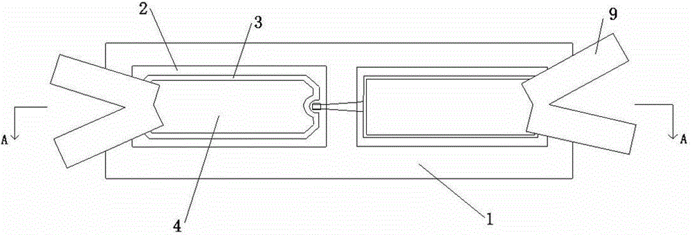
[0023] Such as figure 2 As shown, a multi-beam leaded GaAs-based Schottky frequency-multiplier diode includes a GaAs-based Schottky frequency-multiplier diode body, and both ends of the GaAs-based Schottky frequency-multiplier diode body are provided with The multi-beam lead 9, the composition of the multi-beam lead 9 is gold. The multi-beam lead 9 includes two beam-type sub-leads connected together at one end, each beam-type sub-lead is in the shape of a cuboid, and the two beam-type sub-leads are located on the same horizontal plane. The thickness of the beam-type sub-leads is 2 μm-4 μm, the length is 75 μm-150 μm, and the angle between the outermost two beam-type sub-leads is 30°-60°.

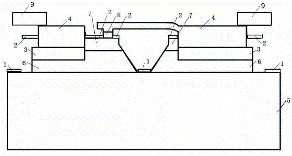
[0024] Such as image 3 As shown, the GaAs-based Schottky frequency multiplier diode body includes a semi-insulating substrate layer 5, a passi...


PUM

PropertyMeasurementUnit
Thicknessaaaaaaaaaa
Angleaaaaaaaaaa
Lengthaaaaaaaaaa

Abstract

The invention discloses a gallium arsenide-based Schottky frequency-doubling diode with multi-beam leads and relates to the technical field of semiconductor devices. The gallium arsenide-based Schottky frequency-doubling diode comprises a gallium arsenide-based Schottky frequency-doubling diode body. The multi-beam type leads are disposed at two ends of the gallium arsenide-based Schottky frequency-doubling diode body. Each multi-beam type lead comprises at least two beam type sub-leads with one ends connected, and the thickness of each beam type sub-lead is 2-4 micrometers. The gallium arsenide-based Schottky frequency-doubling diode has the advantages that the fact that the gallium arsenide-based Schottky frequency-doubling diode is normally mounted on a circuit is guaranteed, the safety and reliability of the Schottky frequency-doubling diode are increased, high mounting yield is achieved, mounting quality is guaranteed, production and scientific research costs are lowered greatly, the diode is simple in structure and convenient to use, and the service life of the diode is prolonged.

Description

technical field [0001] The invention relates to the technical field of semiconductor devices. Background technique [0002] Terahertz (THz) waves refer to electromagnetic waves with a frequency in the range of 0.3-3THz. The generalized terahertz wave frequency refers to 100GHz to 10THz, where 1THz=1000GHz. THz waves occupy a very special position in the electromagnetic spectrum, and THz technology is recognized as a very important cross-frontier field by the international scientific and technological community. [0003] In the low-end range of THz frequency, the solid-state source is usually obtained by frequency doubling of semiconductor devices. This method doubles the frequency of the millimeter wave to the THz frequency band through a nonlinear semiconductor device, and has the advantages of compact structure, easy adjustment, long life, controllable waveform, and normal temperature operation. At present, short-wavelength submillimeter wave and THz solid-state sources ...

Claims


Application Information

Patent Timeline
IPC IPC(8): H01L29/872H01L23/49
CPCH01L24/46H01L29/872H01L23/49H01L2224/46
Inventor 王俊龙邢东梁士雄张立森杨大宝赵向阳冯志红
Owner THE 13TH RES INST OF CHINA ELECTRONICS TECH GRP CORP
Why Eureka
Try Eureka