Semiconductor drive device and power conversion device using same

A drive device and semiconductor technology, applied in the direction of output power conversion device, circuit device, emergency protection circuit device, etc., can solve the problems of large detection delay, inability to protect, and inability to effectively use the high-speed detection of emitter current to achieve false positives. Effects with low probability of detection

Active Publication Date: 2015-07-22
HITACHI LTD
View PDF9 Cites 9 Cited by
  • Summary
  • Abstract
  • Description
  • Claims
  • Application Information

AI Technical Summary

Problems solved by technology

[0046] For example, in , when the emitter current detection method and the collector voltage detection method are used together, the detection delay of the collector voltage detection is larger than that of the emitter current detection. In the "AND" operation method, Cannot take advantage of the high speed of emitter current detection
As a result, there is a possibility that Type II short circuit and Type III short circuit that require high speed cannot be protected.

Method used


Image

  • Semiconductor drive device and power conversion device using same
  • Semiconductor drive device and power conversion device using same
  • Semiconductor drive device and power conversion device using same

Examples


Embodiment 1

[0113] [Structure of semiconductor drive device]

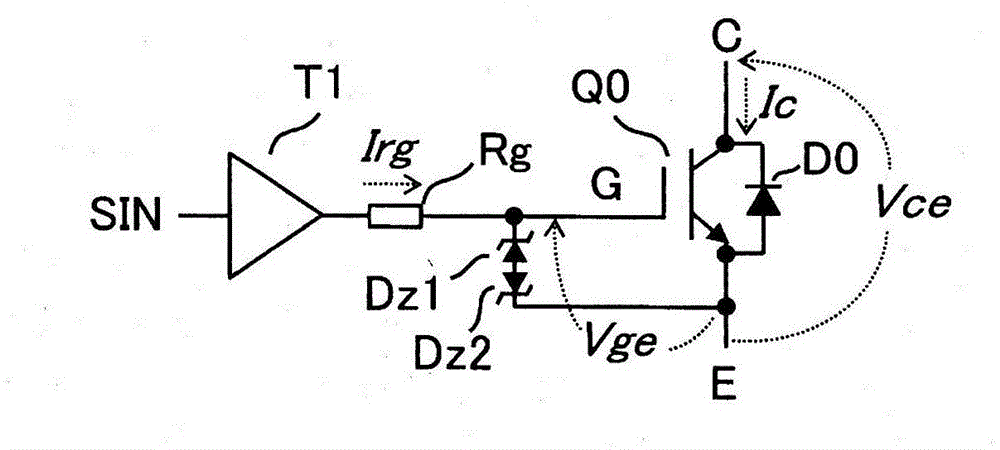
[0114] image 3 It is a diagram showing the basic configuration of the semiconductor drive device according to the first embodiment of the present invention. In addition, in Embodiment 1, an IGBT was taken as an example of a semiconductor for description, but the present invention is not limited thereto, and can be applied to other common semiconductor drive devices.

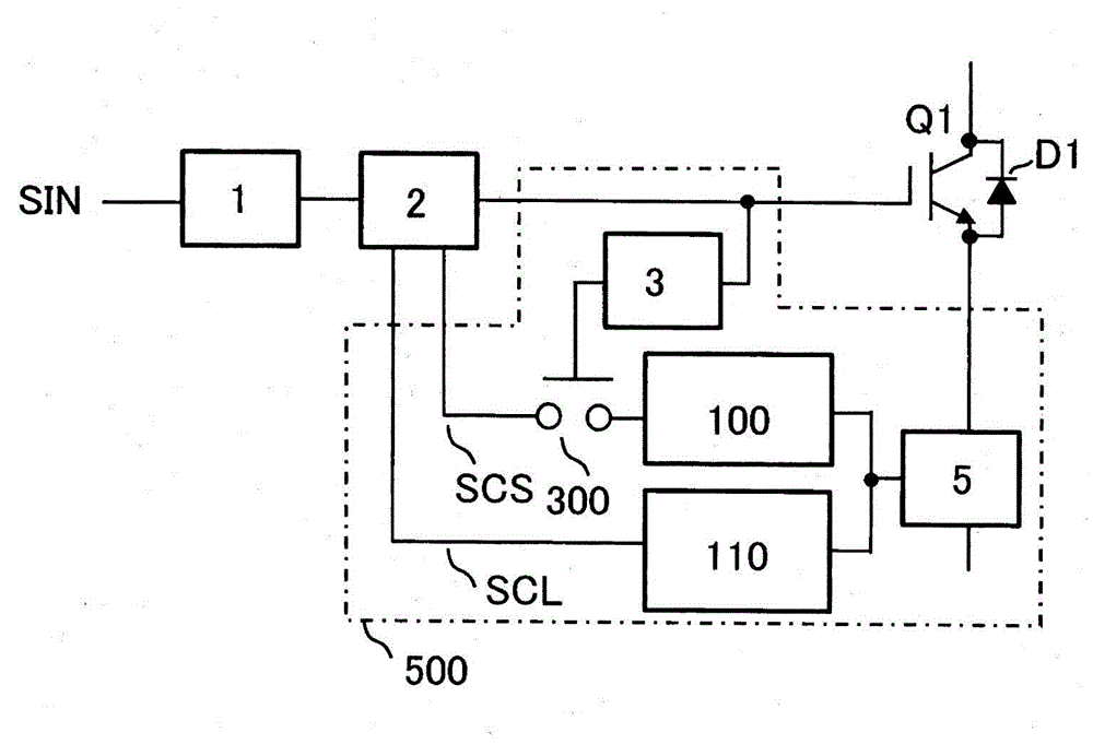
[0115] like image 3 As shown, the semiconductor drive device according to Embodiment 1 is composed of a command unit 1, a gate drive unit 2, a gate voltage detection unit 3, a collector current detection unit 5, a first integration circuit 100, a second integration circuit 110, and an output The control circuit 300 is configured.

[0116] As a configuration example of the collector current detection unit 5, it generally corresponds to a detection resistor, a detection element, or other current detectors.

[0117] The integrating circuit 100 and the integrat...

specific example 1

[0141] Figure 4 yes means image 3 A diagram showing the device configuration of Specific Example 1 of Example 1.

[0142] The gate voltage detection unit 3 detects a gate voltage higher than the power supply voltage using a comparator or the like, and generates a constant-period pulse when abnormality is detected.

[0143] On the other hand, the collector current detection unit 5 obtains the collector current by integrating the induced voltage Le·dIc / dt generated in the parasitic inductance Le of the module, and judges an overcurrent higher than a predetermined value by a comparator circuit. state.

[0144] The integrating circuit 100 and the integrating circuit 110 are constituted by CR filter circuits. The output control circuit 300 is constituted by an AND circuit, and when an abnormality is detected by the gate voltage detection unit 3 , the output of the integration circuit 100 , that is, the detection signal SCS with a short time constant is enabled.

[0145] The g...

specific example 2

[0147] Figure 5 yes means image 3 A diagram showing the device configuration of Specific Example 2 of Example 1.

[0148] and Figure 4 The specific example 1 shown is different in that an operational amplifier is used as the integrating circuit 100 and integrating circuit 110 to obtain the charge amount ∫dt·Ic flowing to the element at the time of short circuit.

[0149] Thus, compared with the time-integration method performed by the CR filter circuit as in Specific Example 1, since it is possible to obtain how much charge flows and set a judgment level corresponding to the accumulated stress, it is possible to realize Reliable design of component loads.


PUM


Abstract

A semiconductor drive device and a power conversion device each having a short circuit protection function that suppresses false detection and is high in reliability are realized. A semiconductor drive device includes: a semiconductor element (Q1) having a pair of main terminals, and a control terminal that controls a current flowing in the main terminal pair; a main detection unit (5) that detects a current or a voltage in the main terminals; an auxiliary detection unit (3) that detects any one of a current or a voltage of the control terminal, or a current or a voltage of the main terminals which is not detected by the main detection unit (5); an integration unit (100,110) that receives an output of the main detection unit (5) to conduct two time integrations different in time constant; and an output control unit (300) that controls an output from the integration unit (100) which is shorter in the time constant according to an output of the auxiliary detection unit (3), in which the voltage or the current of the control terminal is controlled according to an output of the integration unit (110) which is longer in the time constant or an output of the output control unit (300).

Description

technical field [0001] The present invention relates to a semiconductor drive device equipped with a protection function, and a power conversion device using the semiconductor drive device. Background technique [0002] A power conversion device including an inverter realizes power conversion by switching operations of semiconductor switching elements. As typical examples of such semiconductor switching elements, voltage-driven semiconductor elements such as MOS-FETs and IGBTs are widely used. In particular, IGBTs capable of high-speed switching and high power control are used in a wide range of fields, from small-capacity inverters for home appliances to large-capacity inverters for railways. [0003] In order to control such a semiconductor switching element, a semiconductor driver is required. Generally, a driving device for a voltage-driven semiconductor has a function of controlling the conduction state of the semiconductor switching element by applying a voltage to t...

Claims


Application Information

Patent Timeline
Patent Type & Authority Applications(China)
IPC IPC(8): H02M1/08H02M1/32H02H7/20H02H9/02
CPCH03K2217/0027H02M1/32H03K17/0828H02M1/38H02M1/0009
Inventor 恩田航平坂野顺一河野恭彦石川胜美
Owner HITACHI LTD
Why Eureka
Try Eureka