Multiplex pixel element control circuit for super-large planar array tiled CMOS (complementary metal oxide semiconductor) image sensor

An image sensor and control circuit technology, applied in image communication, television, electrical components, etc., can solve problems such as insurmountable inability to reuse, and achieve excellent scalability and reusability, reliable control, and simplified circuit structure. Effect

Active Publication Date: 2015-07-22
NO 771 INST OF NO 9 RES INST CHINA AEROSPACE SCI & TECH
View PDF5 Cites 12 Cited by
  • Summary
  • Abstract
  • Description
  • Claims
  • Application Information

AI Technical Summary

Problems solved by technology

At present, the pixel row control circuit for controlling the row windowing in the image sensor generally adopts the traditional decoding circuit, which is difficult to overcome the disadvantage

Method used


Image

  • Multiplex pixel element control circuit for super-large planar array tiled CMOS (complementary metal oxide semiconductor) image sensor
  • Multiplex pixel element control circuit for super-large planar array tiled CMOS (complementary metal oxide semiconductor) image sensor
  • Multiplex pixel element control circuit for super-large planar array tiled CMOS (complementary metal oxide semiconductor) image sensor

Examples


Example Embodiment

[0023] Examples:

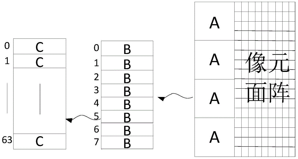
[0024] A multiplexed pixel control circuit used for super-large area array splicing CMOS image sensor to generate 4k*4k pixel area array row control signal. The pixel structure is 2.5T, and each 1K row circuit is required to be multiplexed and the minimum The window size is 128*128. The scheme of the embodiment is as figure 1 Shown. The present invention includes 4 levels of serial pixel control subcircuit A, each level of serial pixel control subcircuit A generates control signals of 1024 rows of pixels, and each serial pixel control subcircuit A is the smallest reusable unit. Among them, the serial pixel control sub-circuit A includes an 8-level serial pixel control sub-circuit B and a window address gating circuit. The pixel control sub-circuit B generates control signals of 128 rows of pixels, and each pixel controls the sub-circuit Circuit B is a basic windowing unit, including 64-level minimum pixel control sub-circuit C.
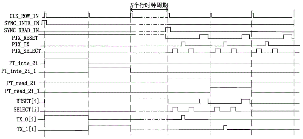
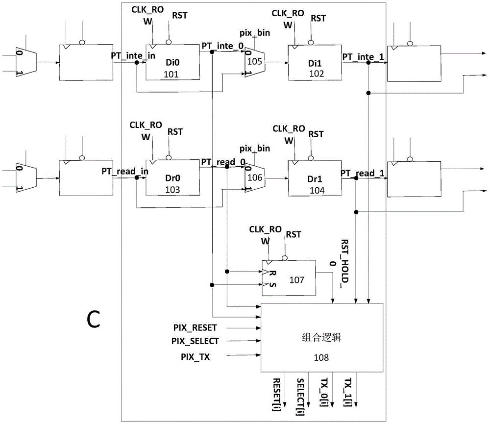
[0025] The multiplexed pixel c...


PUM


Abstract

The invention discloses a multiplex pixel element control circuit for a super-large planar array tiled CMOS (complementary metal oxide semiconductor) image sensor. The multiplex pixel element control circuit comprises L levels of serial pixel element control sub-circuits A. Each level of serial pixel element control sub-circuits A can generate a control signal of I rows of pixel elements. Each serial pixel element control sub-circuit A comprises K levels of serial pixel element control sub-circuits B and a windowing address strobe circuit. Each serial pixel element control sub-circuit B comprises W levels of smallest pixel element sub-circuits C. By designing the windowing address strobe circuits, except the difference of I/O bonding finger area lead connection modes, the L serial pixel element control sub-circuits A have completely uniform address-coding structures, thus a windowing function of the circuit is achieved. The circuit is simple in structure, reliable to control, good in extensibility and reusability and applicable to CMOS image sensor chip circuits of different planar array scales.

Description

technical field [0001] The invention belongs to the technical field of CMOS image sensors, and in particular relates to a multiplexed pixel control circuit for splicing CMOS image sensors with super large area arrays. Background technique [0002] The role of the image sensor is mainly to collect digital images and convert the collected optical signals into electrical signals. Image sensors that have been commercially available on a large scale are mainly divided into two types: CCD and CMOS. Compared with CCD image sensors, CMOS image sensors have the advantages of low power consumption, low cost and high compatibility, and are widely used in the fields of aerospace, biotechnology and consumer electronics. [0003] With the expansion of the application range, consumers have higher requirements for image size, and the demand for large-scale image sensors is increasing. Traditional image sensor design methods often only focus on improving resolution or frame rate, ignoring ...

Claims


Application Information

Patent Timeline
IPC IPC(8): H04N5/374H04N5/353H04N5/378
Inventor 张先娆汪西虎徐晚成张曼
Owner NO 771 INST OF NO 9 RES INST CHINA AEROSPACE SCI & TECH
Why Eureka
Try Eureka