Pixel combination circuit in reading circuit and pixel combination implementation method of pixel combination circuit

A readout circuit and pixel technology, which is applied in the field of image sensors, can solve problems such as process influence, noise contribution cannot be eliminated, and influence on the swing of pixel column line, etc., to achieve mature technology, improve output accuracy, and high adjustment degree Effect

Active Publication Date: 2015-07-22
NO 771 INST OF NO 9 RES INST CHINA AEROSPACE SCI & TECH
View PDF4 Cites 4 Cited by
  • Summary
  • Abstract
  • Description
  • Claims
  • Application Information

AI Technical Summary

Problems solved by technology

[0004] However, there are also defects in the physical merging of pixels. The schematic diagram of the 2×1 charge merging circuit in a pixel is shown in image 3 As shown, this method of pixel merging is realized by averaging the photogenerated charges of the two columns in the pixel unit, which will not only reduce the pixel fill factor but also affect the output swing of the pixel column line, FD point capacitance Significantly affected by the process, the combined results are difficult to achieve high-precision averaging. At the same time, the contribution of clock feedthrough and charge injection introduced by the combined switch to noise cannot be eliminated.

Method used


Image

  • Pixel combination circuit in reading circuit and pixel combination implementation method of pixel combination circuit
  • Pixel combination circuit in reading circuit and pixel combination implementation method of pixel combination circuit
  • Pixel combination circuit in reading circuit and pixel combination implementation method of pixel combination circuit

Examples


Embodiment Construction

[0040] The present invention will be further described in detail below in conjunction with the accompanying drawings.

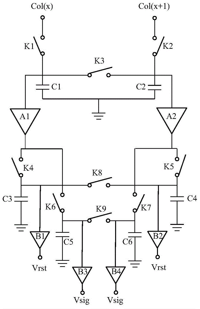
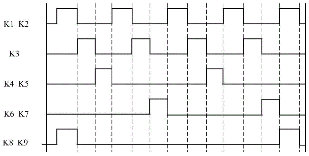
[0041] see Figure 1-7, the present invention includes a first switch K1, a second switch K2, a third switch K3, a fourth switch K4, a fifth switch K5, a sixth switch K6, a seventh switch K7, an eighth switch K8, a ninth switch K9, a processing circuit A1, a second processing circuit A2, a first buffer B1, a second buffer B2, a third buffer B3, and a fourth buffer B4; the input terminals of the first switch K1 and the second switch K2 are respectively connected to Any two adjacent columns of pixel signal output terminals; the output terminals of the first switch K1 and the second switch K2 are respectively connected to the input terminals of the first capacitor C1 and the second capacitor C2; the outputs of the first capacitor C1 and the second capacitor C2 The terminals are grounded or fixed level; the input terminal of the first processing circuit A1 is co...


PUM


Abstract

The invention relates to a pixel combination circuit in a reading circuit and a pixel combination implementation method of the pixel combination circuit. Control is achieved by setting a third switch, an eighth switch and a ninth switch, when the three switches are on, the charges of a first capacitor and a second capacitor, a third capacitor and a fourth capacitor, and a fifth capacitor and a sixth capacitor are averaged, that is to say two lines of input / output signals are averaged, signal average values are output by setting an output control switch, and pixel combination purpose is achieved. When input pixel combination technology is used to average the charges of the sampling capacitors, sampling capacitance is doubled, so that the pixel combination circuit tends to use output pixel combination which does not introduce extra capacitance; due to the fact that output sampling capacitance is large, influence of small capacitor mismatch on output after averaging can be neglected, and the combination does not influence final output precision.

Description

technical field [0001] The invention belongs to the field of image sensors, and in particular relates to a pixel merging circuit in a readout circuit and a method for realizing the pixel merging. Background technique [0002] Solid-state image sensors are mainly divided into two types: CCD (Charge-coupled Device) and CMOS (Complementary Metal-Oxide semiconductor) according to the different components. Their functions show more changes with the change of the application environment. The purpose of pixel merging is to On the basis of reducing the spatial resolution, the sensitivity of the light detector to light is enhanced, the data processing amount is reduced, the data processing speed is improved, and the system power consumption is reduced. The ways of realizing pixel merging can be divided into two categories according to different implementation methods: pixel merging on physical structure and sub-sampling technology. The sub-sampling technology reads out part of the p...

Claims


Application Information

Patent Timeline
IPC IPC(8): H04N5/378
Inventor 何杰吴龙胜郭仲杰李栋肖筱
Owner NO 771 INST OF NO 9 RES INST CHINA AEROSPACE SCI & TECH
Why Eureka
Try Eureka