Check patentability & draft patents in minutes with Patsnap Eureka AI!

Array substrate and display device

An array substrate and substrate technology, applied in nonlinear optics, instruments, optics, etc., can solve the problems of reducing transmittance, increasing process time, increasing device thickness, etc., to achieve the effect of improving production efficiency and reducing process processes

Active Publication Date: 2015-07-29
XIAMEN TIANMA MICRO ELECTRONICS +1
View PDF8 Cites 25 Cited by
  • Summary
  • Abstract
  • Description
  • Claims
  • Application Information

AI Technical Summary

Problems solved by technology

[0005] However, the array substrate of the touch display device in the prior art needs to separately arrange the touch wiring, which increases the thickness of the device, reduces the transmittance and increases the time of the manufacturing process.

Method used


Image

  • Array substrate and display device
  • Array substrate and display device
  • Array substrate and display device

Examples


Embodiment Construction

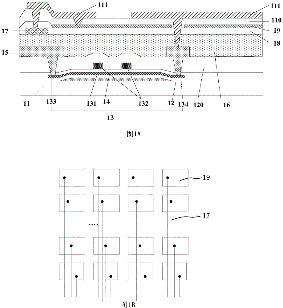
[0040] The present invention will be further described in detail below in conjunction with the accompanying drawings and embodiments. It should be understood that the specific embodiments described here are only used to explain the present invention, but not to limit the present invention. In addition, it should be noted that, for the convenience of description, only some structures related to the present invention are shown in the drawings but not all structures.

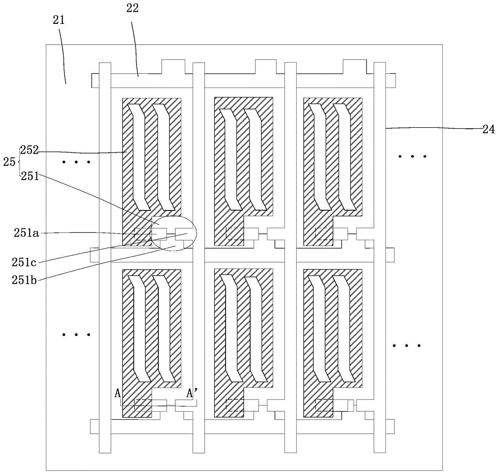
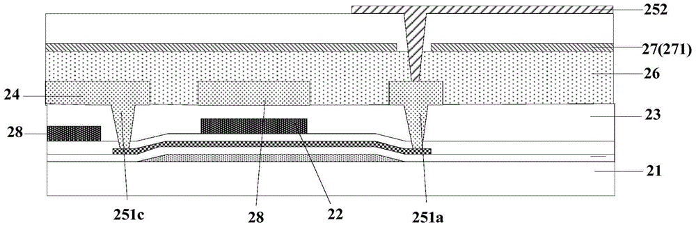
[0041] Figure 2A A top view of an array substrate provided in an embodiment of the present invention, combined with Figure 2B , Figure 2B for Figure 2A The sectional view along the A-A' direction of the array substrate shown, such as Figure 2A and Figure 2B As shown, the array substrate specifically includes:

[0042] Substrate 21;

[0043] A first metal layer disposed on the substrate 21, the first metal layer adopts a patterning process to form a plurality of scanning lines 22, and the plurality of s...


PUM

PropertyMeasurementUnit
thicknessaaaaaaaaaa

Abstract

The invention discloses an array substrate and a display device. The array substrate comprises a substrate, a plurality of scanning lines, a first insulation layer, a plurality of data lines, a plurality of pixel units, a common electrode layer and a plurality of touch electrode wires, wherein the plurality of scanning lines are arranged on the substrate and extend in a first direction; the first insulation layer is arranged on the plurality of scanning lines; the plurality of data lines are arranged on the first insulation layer and extend in a second direction; the plurality of pixel units are arrayed to form a matrix and comprise transistor switches and pixel electrodes; the common electrode layer comprises a plurality of touch electrodes; the plurality of touch electrode wires are connected to the corresponding touch electrodes respectively, and at least partial touch electrode wires are arranged on the same layer with the scanning lines or the data lines; the touch electrode wires are connected with the corresponding touch electrodes respectively through first connection structures. The touch electrode wires are arranged on the same layer with the scanning lines or the data lines so that the metal manufacturing procedure is omitted and the production efficiency can be improved.

Description

technical field [0001] Embodiments of the present invention relate to the technical field of liquid crystal displays, and in particular, to an array substrate and a display device. Background technique [0002] Liquid crystal display, commonly known as LCD (Liquid Crystal Display) in English, is a kind of flat-panel display. With the development of science and technology, LCD is also developing towards the goal of being light, thin, short, and small. Whether it is a wide viewing angle display, low power consumption, small size, or zero radiation, etc., users can enjoy the best Visual effects. [0003] A display with a touch function is produced based on a function-enriching technology. Common touch technologies include In-cell touch technology and On-cell touch technology. Among them, the In-cell touch technology refers to the technology of embedding the touch panel function inside the liquid crystal display panel, and the On-cell touch technology refers to the technology ...

Claims


Application Information

Patent Timeline
Patent Type & Authority Applications(China)
IPC IPC(8): G02F1/1333G02F1/1343
CPCG02F1/13338G02F1/1343G02F1/136227G02F1/136286
Inventor 彭涛崔萌王慧敏
Owner XIAMEN TIANMA MICRO ELECTRONICS
Features
  • R&D
  • Intellectual Property
  • Life Sciences
  • Materials
  • Tech Scout
  • Unparalleled Data Quality
  • Higher Quality Content
  • 60% Fewer Hallucinations
Learn More