
Display panel

A display panel and display layer technology, applied in optics, instruments, electrical components, etc., can solve problems such as disconnection, easy chamfering, complex structure and manufacturing process, etc.

Active Publication Date: 2015-08-12
INNOLUX CORP
View PDF4 Cites 5 Cited by
  • Summary
  • Abstract
  • Description
  • Claims
  • Application Information

AI Technical Summary

Problems solved by technology

[0003] However, with the development of high-resolution display panels, their structures and manufacturing processes are becoming more complex, and there may be more than one insulating layer between different conductive layers.
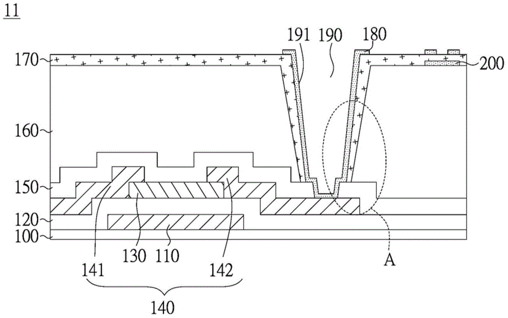
Due to the different film forming conditions of different insulating layers, it is easy to form chamfers when etching to form through holes
Such chamfering can easily lead to incomplete filling of the through hole, or disconnection when the conductive layer is plated, which affects the quality of the display panel

Method used


Image

  • Display panel
  • Display panel
  • Display panel

Examples


Embodiment Construction

[0043] Embodiments of the present invention will be described in detail below with reference to the accompanying drawings. The same reference numerals are used in the drawings to designate the same or similar parts. It should be noted that the drawings have been simplified to clearly illustrate the content of the embodiments, and the size ratios in the drawings are not drawn to the same scale as the actual product, so they are not used to limit the protection scope of the present invention.

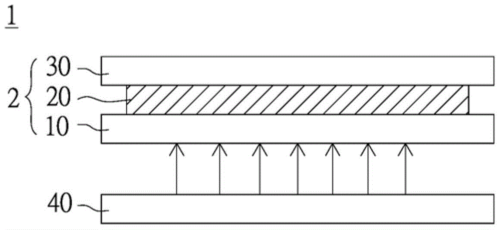
[0044] Please refer to figure 1 , which shows a display device according to an embodiment of the present invention. The display device 1 includes a display panel 2 and a backlight module 40 . When the display panel 2 is a liquid crystal display panel, it is composed of a thin film transistor substrate 10 , a display layer 20 and an opposite substrate 30 , and the display layer is a liquid crystal layer. The display layer 20 is located between the TFT substrate 10 and the opposite subst...


PUM


Abstract

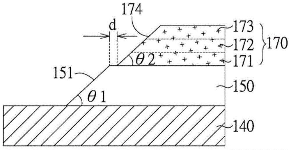
The invention discloses a display panel. A film transistor substrate of the display panel comprises a bottom plate, a gate layer, a gate dielectric layer, a semiconductor layer, a first electrode layer, a first passivation layer, a second passivation layer, a via hole and a second electrode layer. The gate layer is located on the substrate. The gate dielectric layer is located on the gate layer. The semiconductor layer is located on the gate dielectric layer. The first electrode layer is located on the semiconductor layer. The first passivation layer is located on the first electrode layer. The second passivation layer is located on the first passivation layer. The via hole penetrates the first passivation layer and the second passivation layer to expose part of the first electrode layer. The second electrode layer is electrically connected with the first electrode layer through the via hole. The first passivation layer is provided with a first tilt angle on a side edge of the via hole, the second passivation layer is provided with a second tilt angle on a side edge of the via hole, and the angle difference between the first tilt angle and the second tilt angle is less than 30 degrees.

Description

technical field [0001] The present invention relates to a display panel, and in particular to a display panel with a thin film transistor substrate. Background technique [0002] In the manufacturing process of the display panel, if the conductive layers on the upper and lower sides of the insulating layer are to be conducted, a via or contact hole is designed so that the conductive layers on the upper and lower sides can be electrically connected. For example, the method of electrically connecting the pixel electrode and the drain of the thin film transistor in the pixel structure is to perform a patterning process before forming the pixel electrode to form a via hole in the insulating layer to expose the underlying drain, and then After the pixel electrode is plated, the pixel electrode and the drain can be electrically connected through the through hole. [0003] However, with the development of high-resolution display panels, their structures and manufacturing processes...

Claims


Application Information

Patent Timeline
Patent Type & Authority Applications(China)
IPC IPC(8): H01L27/32G02F1/136
Inventor 李冠锋林明昌颜子旻
Owner INNOLUX CORP
Learn More