Electric field regulating antiferromagnetic base Hall device and preparation method thereof

A Hall device and electric field regulation technology, applied in the field of electronic devices, can solve the problems of difficult control, limit the practical process, etc., achieve the effect of clear interface, insensitive to external magnetic field and thermal disturbance, and reduce interference

Active Publication Date: 2015-07-01
TSINGHUA UNIV
View PDF1 Cites 7 Cited by
  • Summary
  • Abstract
  • Description
  • Claims
  • Application Information

AI Technical Summary

Problems solved by technology

Since the magnetic moments of antiferromagnetic materials are arranged antiparallel and the net magnetic moment is zero, it is very difficult to manipulate it, which limits the practical process

Method used


Image

  • Electric field regulating antiferromagnetic base Hall device and preparation method thereof
  • Electric field regulating antiferromagnetic base Hall device and preparation method thereof

Examples


Embodiment 1

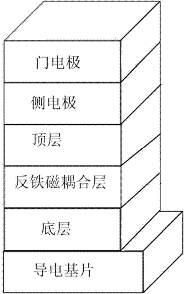
[0049] Embodiment 1, preparation Y 3 Fe 5 o 12 / IrMn / HfO 2 / Hall device with ionic liquid structure

[0050] Preparation of Hall device:

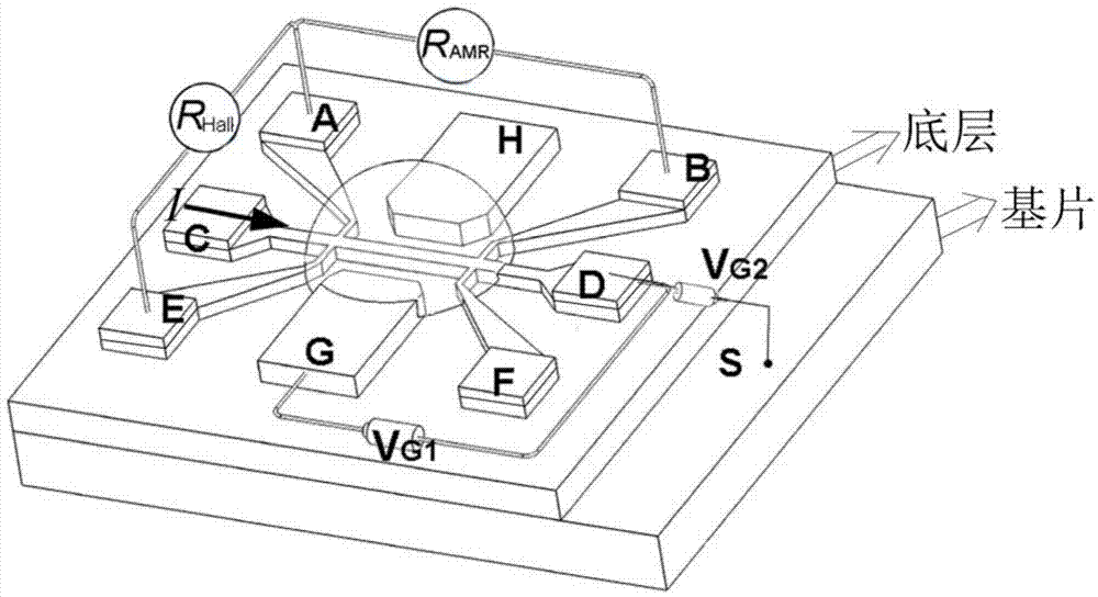
[0051] (1) Doping SrTiO in Nb 3 A 500 μm wide side is reserved on the edge of the substrate, and 50 nm of yttrium iron garnet (Yttrium iron garnet (Y 3 Fe 5 o 12 ), marked S on the side, for test wiring. (2) In the bottom layer Y 3 Fe 5 o 12 Coat the photoresist of type AZ5214E, then use ultraviolet exposure to make the pattern of the Hall device, and sequentially deposit a 5nm antiferromagnetic coupling layer IrMn and a 2nm top layer of hafnium dioxide (HfO 2 ), and then use acetone to remove the glue, and use a lift-off process to obtain a part of the Hall device. The area of ​​the square where the top layer is located is 2000×2000 μm 2 , the area of ​​the overlapped part of the center of the two cross-shaped structures in the middle is 40×30 μm 2 . (3) if figure 2 As shown, 20nm Ti and 80nm Au were deposited by electron...

Embodiment 2

[0054] Embodiment 2, preparation BiFeO 3 / FeRh / HfO 2 / Hall device with ionic liquid structure

[0055] Preparation of Hall device:

[0056] (1) in SrRuO 3 A 500μm wide side is left on the side of the substrate, and 100nm BiFeO is deposited by masking 3 , marked S on the side, for test wiring. (2) On the underlying BiFeO 3 Coat the photoresist of model AZ5214E, then use ultraviolet exposure to make the pattern of Hall device, and deposit 20nm antiferromagnetic coupling layer FeRh and 2nm top layer HfO in sequence 2 , and then use acetone to remove the glue, and use a lift-off process to obtain a part of the Hall device. The area of ​​the square where the top layer is located is 1000×1000 μm 2 , the area of ​​the overlapped part of the center of the two cross-shaped structures in the middle is 20×15 μm 2 . (3) The eight square electrodes of A, B, C, D, E, F, G, and H are plated with a Ti layer of 20nm and an Au layer of 80nm by electron beam evaporation by ultraviolet ...

Embodiment 3

[0059] Embodiment 3, PZT / [Co / Pt] / IrMn / HfO 2 / Hall device with ionic liquid structure

[0060] Preparation of Hall device:

[0061] (1) in SrRuO 3 A side with a width of 500 μm is reserved on the side of the substrate, and 50 nm of PZT is deposited by using a mask, and the side is marked as S for testing wiring. (2) Coat the photoresist type AZ5214E ​​on the underlying PZT, then use ultraviolet exposure to make the pattern of the Hall device, and deposit the antiferromagnetic coupling layer [Co / Pt] in sequence 5 / IrMn and 2nm top HfO 2 , where the thickness of Co is 0.6nm, the thickness of Pt is 1nm, and the thickness of IrMn is 3nm. Afterwards, acetone was used to remove the glue, and a part of the Hall device was obtained by a lift-off process. The area of ​​the square where the top layer is located is 2000×2000 μm 2 , the area of ​​the overlapped part of the center of the two cross-shaped structures in the middle is 40×30 μm 2 . (3) The eight square electrodes of A,...


PUM


Abstract

The invention discloses an electric field regulating antiferromagnetic base Hall device and a preparation method thereof. The electric field regulating antiferromagnetic base Hall device comprises a bottom layer, an antiferromagnetic coupling layer and a top layer deposited on a conductive substrate in sequence, and the top layer is provided with a side electrode and a gate electrode in sequence; the bottom layer is a magnetic insulator layer or a nonmagnetic insulator layer; the bottom layer is a composite layer composed of the magnetic insulator layer or nonmagnetic insulator layer; the antiferromagnetic coupling layer is an antiferromagnetic layer or composed of the antiferromagnetic layer and a ferromagnetic layer; the top layer is a hafnium oxide layer, an aluminum oxide layer or a silicon dioxide layer; the side electrode is a double-layer film composed of a Ti layer and an Au layer or a double-layer film composed of a Ti layer and a Pt layer, and the Ti layer, Au layer or Ti layer and Pt layer are arranged on the top layer in sequence; the gate electrode is ion liquid. The electric field regulating antiferromagnetic base Hall device is simple in structure, easy to prepare, low in cost and good in magnetization characteristic, and the electric field regulating antiferromagnetic base Hall device can serve as a magnetic field detector; the electric field regulating antiferromagnetic base Hall device is nonsensitive to external magnetic field and thermal disturbance, and the measured Hall resistance is more precise; the electric field regulating antiferromagnetic base Hall device is a low-energy consumption spinning device, and the electric field regulating antiferromagnetic base Hall device is significant for the development of antiferromagnetic spinning electronic devices.

Description

technical field [0001] The invention relates to an antiferromagnetic-based Hall device regulated by an electric field and a preparation method thereof, belonging to the field of electronic devices. Background technique [0002] Antiferromagnetic-based spintronics devices have gradually developed into a new research direction due to their potential application value in ultrafast and ultrahigh-density spintronics devices, and have aroused extensive research interests. Since the discovery of exchange bias in 1957, antiferromagnetic materials have been used as an important static support material to pin ferromagnetic layers and have been widely used in spin valve and tunnel junction devices. With the functionalization of antiferromagnetic materials in recent years, people have begun to try to store information by manipulating the magnetic moment of antiferromagnetism, and have developed new device configurations such as antiferromagnetic memristors and antiferromagnetic Tunnel ...

Claims


Application Information

Patent Timeline
Patent Type & Authority Applications(China)
IPC IPC(8): H01L43/06H01L43/14
Inventor 王钰言宋成潘峰
Owner TSINGHUA UNIV
Why Eureka
Try Eureka