Chip scale packaging method and structure for light-emitting device

A chip-level packaging and light-emitting device technology, applied in the direction of electric solid-state devices, semiconductor devices, electrical components, etc., can solve the problems of increasing production process and cost, unfavorable product miniaturization, unfavorable chip heat dissipation, etc., to ensure color temperature uniformity, Convenience for end users and simplification of manufacturing process

Active Publication Date: 2015-08-19
湖南省日晶照明科技有限责任公司
View PDF6 Cites 25 Cited by
  • Summary
  • Abstract
  • Description
  • Claims
  • Application Information

AI Technical Summary

Problems solved by technology

This packaging method requires an additional supporting substrate, which increases the production process and cost, and also increases the thermal resistance, which is not conducive

Method used


Image

  • Chip scale packaging method and structure for light-emitting device
  • Chip scale packaging method and structure for light-emitting device
  • Chip scale packaging method and structure for light-emitting device

Examples


Embodiment 1

[0045] Such as Figure 10 As shown, a method for chip-scale packaging of light-emitting devices provided in this embodiment is used for packaging of light-emitting devices that do not need to be converted into white light, including steps:

[0046]Step 101: Arranging at least one flip-chip light-emitting device equidistantly on the conversion base film, the main light-emitting surface of the flip-chip light-emitting device is away from the conversion base film, wherein the surface of the conversion base film has a certain viscosity and is durable High temperature, used for adhering the flip-chip light-emitting devices; equidistant in the present invention means that the arrangement distances of multiple flip-chip light-emitting devices in the x-axis and y-axis directions are equal. Here, the conversion base film needs to be resistant to a high temperature of at least 150°C, depending on the nature of the conversion base film. Step 102: Form dams between and / or around the flip...

Embodiment 2

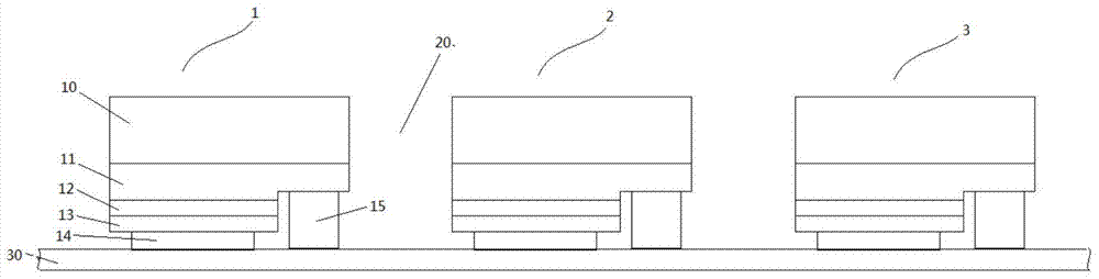
[0062] On the basis of Example 1, combined with Figure 1 to Figure 5 as well as Figure 10 The present invention is described in detail:

[0063] The LED chip of the flip-chip structure comprises a substrate 10, a first semiconductor layer 11, an active region 12 and a second semiconductor layer 13, and the second electrode 14 and the first electrode 15 are connected with the second semiconductor layer 13 and the first semiconductor layer 11 respectively. electrical connection. The conductivity types of the first semiconductor layer 11 and the second semiconductor layer 13 are opposite. The first electrode 15 and the second electrode 14 can comprise multiple layers or a single layer, which include a conductive material layer with high reflectivity, such as a conductive layer made of high reflectivity metals such as Ag, Ru, Al, or a high-transmittance conductive layer. Composite optical film composed of film and highly reflective multilayer dielectric film.

[0064] Multip...

Embodiment 3

[0072] On the basis of embodiment one and two, combine Figure 6 to Figure 8B , provides another example:

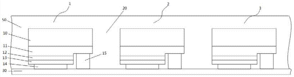
[0073] like Figure 6 As shown, on the basis of the second embodiment, dams are formed between and / or around the flip-chip light-emitting devices on the conversion base film.

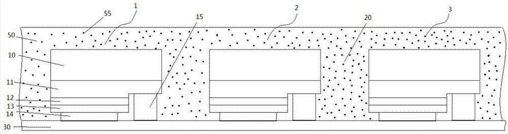
[0074] Specifically: after a plurality of flip chip LED chips 1, 2, 3 are arranged on the conversion base film 30 at a certain interval 20, a "dam" 80 is formed around the LED chips 1-3. The dam 80 can be formed by sticking a film or other methods, and can be a large dam 80 that is only distributed around all chips or some chips (such as Figure 7A shown) can also be multiple grids (such as Figure 7B Shown) structure, but require the height of the dam 80 to be uniform.

[0075] Apply the prepared encapsulation glue 50 evenly in the dam without air bubbles. The encapsulation glue 50 coated above and around the LED chips 1 - 3 is separated by the dam 80 . The height of the dam 80 exceeds the ...


PUM

PropertyMeasurementUnit
Thicknessaaaaaaaaaa
Thicknessaaaaaaaaaa
Hardnessaaaaaaaaaa

Abstract

The application discloses a chip scale packaging method for a light-emitting device. The scale packaging method includes steps: at least a flip light-emitting device is arranged on a conversion base film with equal intervals, a main light-outlet surface of the flip light-emitting device is opposite to the conversion base film, dams are formed between the flip light-emitting devices and/or around the flip light-emitting devices on the conversion base film, packaging glue is respectively coated on the flip light-emitting devices and the conversion film, the dams are removed when the packaging glue is cured to be non-liquid, the packaging glue is cut after the packaging glue is completely cured, the conversion base film is removed, and the chip scale packaging structure is obtained after molding. The invention also discloses a chip scale packaging structure for the light-emitting device. According to the chip scale packaging method and the structure for the light-emitting device, packaging process steps of the chip are greatly simplified, a submount of the chip is saved, the cost is lowered, and the work efficiency of users can be more conveniently improved.

Description

technical field [0001] The invention relates to the field of semiconductor packaging, in particular to a chip-level packaging method and packaging structure of a light emitting device. Background technique [0002] From the perspective of the development of LED packaging forms, bullet-type packages were mainly used in the early days. With the demand of the market, different forms of packaging brackets have appeared one after another. For example, surface mount devices (SMD) and high-power integrated package types are most commonly used in the market at present. [0003] The LED chips used in the above-mentioned packages are basically a front-loading structure, and the packaging process involves die bonding, wire bonding, and glue dispensing in the bracket. Then use it as a carrier to paste on the carrier board of the lamp. From the perspective of heat dissipation, the thermal resistance of the system from the chip, the bracket to the lamp carrier is relatively large, whic...

Claims


Application Information

Patent Timeline
IPC IPC(8): H01L33/52H01L33/00
CPCH01L33/52H01L2224/14H01L2933/005
Inventor 王良臣汪延明苗振林梁智勇许亚兵
Owner 湖南省日晶照明科技有限责任公司
Why Eureka
Try Eureka