Antireflection film, manufacturing method therefor, display panel, and display device

An anti-reflection film and display panel technology, which is applied in the field of display panels and display devices, and anti-reflection film, can solve the problems of high cost of anti-reflection film, complex bonding process, and easy generation of static electricity, so as to increase the overall thickness and production cost , The production process is easy to realize, avoiding bad effects

Active Publication Date: 2015-08-26
BOE TECH GRP CO LTD
View PDF9 Cites 4 Cited by
  • Summary
  • Abstract
  • Description
  • Claims
  • Application Information

AI Technical Summary

Problems solved by technology

The bonding process is relatively complicated, and static electricity is likely to be generated during the bonding process, which may break down the electrodes in the flat panel display and cause the flat panel display to be defective; and directly bonding the antireflection film on the flat panel display will increase the overall Thickness; In addition, the cost of the existing anti-reflection film is relatively high, correspondingly, it will increase the production cost of the flat panel display

Method used


Image

  • Antireflection film, manufacturing method therefor, display panel, and display device
  • Antireflection film, manufacturing method therefor, display panel, and display device
  • Antireflection film, manufacturing method therefor, display panel, and display device

Examples


Embodiment Construction

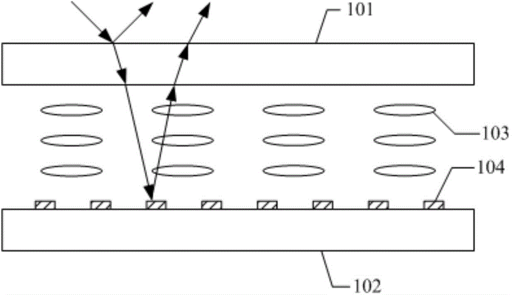
[0037] The specific implementation manners of an anti-reflection film, a manufacturing method thereof, a display panel and a display device provided by the embodiments of the present invention will be described in detail below with reference to the accompanying drawings.

[0038] The shape and thickness of each film layer in the drawings do not reflect their true proportions, but are only intended to schematically illustrate the content of the present invention.

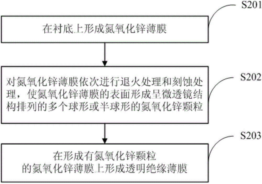
[0039] A kind of manufacturing method of anti-reflection film provided by the embodiment of the present invention, such as figure 2 shown, including the following steps:

[0040] S201, forming a zinc oxynitride film on the substrate;

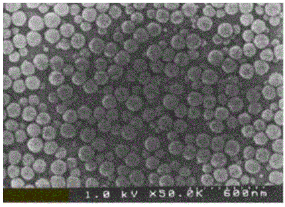
[0041] S202. Perform annealing treatment and etching treatment on the zinc oxynitride film in sequence, so that a plurality of spherical or hemispherical zinc oxynitride particles arranged in a micro-lens structure are formed on the surface of the zinc oxynitride film.

[0042] The ...


PUM

PropertyMeasurementUnit
diameteraaaaaaaaaa
diameteraaaaaaaaaa
diameteraaaaaaaaaa

Abstract

The invention discloses an antireflection film, a manufacturing method therefor, a display panel, and a display device. The method comprises the steps: forming an N-doped zinc oxide film; sequentially carrying out annealing and etching of the N-doped zinc oxide film, and enabling a plurality of spherical or semispherical N-doped zinc oxide particles arranged in a microlens structure to be formed on the surface of the N-doped zinc oxide film; enabling the N-doped zinc oxide film, the surface of which is provided with the plurality of spherical or semispherical N-doped zinc oxide particles arranged in the microlens structure, to serve as the antireflection film, wherein the shape of the N-doped zinc oxide particles in the formed N-doped zinc oxide film is easy to control, and the manufacturing technology is easy to implement. Moreover, the antireflection film can be integrated on the display panel, and there is no need of pasting technology. Not only the overall thickness and manufacture cost of the display panel cannot be increased, but also the display panel can be prevented from becoming bad in a pasting process.

Description

technical field [0001] The invention relates to the field of display technology, in particular to an anti-reflection film, a manufacturing method thereof, a display panel and a display device. Background technique [0002] With the continuous development of display technology, light emitting diode (Light Emitting Diode, LED), organic light emitting diode (Organic Light Emitting Diode, OLED), plasma display (Plasma Display Panel, PDP) and liquid crystal display (Liquid Crystal Display, LCD) etc. Flat panel displays are developing rapidly. [0003] Take the existing LCD as an example for illustration, such as figure 1 As shown, it includes: an opposing substrate 101, an array substrate 102, and a liquid crystal layer 103 between the two substrates; wherein, a metal signal line 104, such as a gate line or a data line, is provided on one side of the array substrate 102. . When the LCD is in the external environment, the natural light in the external environment is incident on...

Claims


Application Information

Patent Timeline
Patent Type & Authority Applications(China)
IPC IPC(8): G02B1/115
CPCG02B1/115G02B1/118Y02E10/52G02B1/113C09K2323/00C09K2323/051H10K50/86H10K50/858H01L31/0543G02B1/12G02F1/133502G02F1/133526G02F2201/38
Inventor 王东方王美丽张立
Owner BOE TECH GRP CO LTD
Why Eureka
Try Eureka