SMD diode preparation technology

A preparation process and technology for diodes, which are used in semiconductor/solid-state device manufacturing, electrical components, circuits, etc., can solve the problems of low curing temperature, affect diode performance, damage, etc., and achieve the effects of enhancing compactness, saving resources, and simplifying the process.

Active Publication Date: 2016-07-20
王志敏
View PDF4 Cites 8 Cited by
  • Summary
  • Abstract
  • Description
  • Claims
  • Application Information

AI Technical Summary

Problems solved by technology

[0009] (1) Since SMD packaging mostly uses GPP chips, and the manufacturing process of GPP chips is relatively complicated, requiring three photoresist developing mask manufacturing processes, and when molding and slicing, there are often tiny cracks caused by cutting, and the edges show 90 The sharp angle shape is easy to be damaged by collision during processing;
[0010] (2) In addition, GPP glass only covers a part of the cutting surface, and cannot cover the entire cutting surface. Because the thickness of the cover glass is very thin, it can only withstand the reverse voltage of less than 1600V;
[0011] (3) In addition, the passivation glass of GPP chips inevitably contains heavy met...

Method used


Image

  • SMD diode preparation technology
  • SMD diode preparation technology
  • SMD diode preparation technology

Examples


Embodiment 1

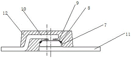
[0049] The chip diode of this embodiment, such as Image 6 As shown, it includes a chip 15, the two ends of the chip are respectively welded with the upper lead 13 and the lower lead 14 by solder 16, and the chip connection end of the lower lead is provided with a pit 19 that can accommodate the chip, so that the inner sidewall of the pit 19 and the An annular gap surrounding the periphery of the chip 15 is formed between the side walls of the chip 15, and the chip sheath sealing glue 17 is filled in the annular gap; a plastic package 18 wrapping the chip 15 and the leads is formed outside the leads by plastic sealing.

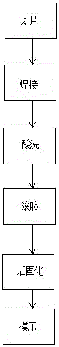
[0050] In this embodiment, the process steps of preparing the chip diode with the above structure are as follows:

[0051] (1) Alloy: take the soldering sheet and diffusion sheet, stack them in the order of soldering sheet → diffusion sheet → soldering sheet, and then place the stacked soldering sheet and diffusion sheet in a high-frequency alloy furnace for a...

Embodiment 2

[0062] Compared with Embodiment 1, this embodiment, in order to form an annular gap around the periphery of the chip outside the chip before the glue filling process in step (6), by changing the structure of Embodiment 1, the soldered leads and the chip Placed in a plastic casing with an open upper end, the specific structure, such as Figure 7 As shown, it includes a chip 15, and the two ends of the chip are respectively welded with an upper lead 13 and a lower lead 14 by solder 16, and the welded chip 15 and the lead are placed in a plastic casing 20 with an upper end opening, so that the plastic casing 20 An annular gap is formed on the periphery of the chip 15 between the inner side wall of the chip 15 and the chip 15, and the chip sheathing glue 17 is filled in the annular gap; The plastic encapsulation structure 18 of the body 20.

[0063] In this embodiment, the process steps of preparing the chip diode with the above structure are as follows:

[0064] (1) Alloy: take...

Embodiment 3

[0074] Compared with Example 1, in order to form an annular gap around the periphery of the chip outside the chip before the glue filling process in step (6), by changing the structure of Example 1, a chip inner shell is prefabricated. The plastic-encapsulated shell of the chip, the soldered leads and the chip are placed in the chip inner shell, the specific structure, such as Figure 8As shown, it comprises a chip 15, and the two ends of the chip are welded with the upper lead 13 and the lower lead 14 respectively by solder 16, and the chip 15 and the lead after welding are placed in the chip inner shell 22, so that the inner side wall of the chip inner shell 22 and the An annular gap on the periphery of the chip 15 is formed between the side walls of the chip 15, and the chip inner shell 22 is arranged at the center of the bottom of a plastic casing 21 whose height is higher than the chip inner shell; and the chip sheath seal glue 17 is filled in the annular gap; And the epo...


PUM


Abstract

The invention relates to an SMD diode preparation technology, and the technology sequentially comprises the steps: scribing, acid pickling, welding, alkaline cleaning, glue pouring, glue curing, plastic packaging, post curing, electroplating, and testing. The technology is advantageous in that the technology employs O/J jacketing for an SMD diode through the adjustment of a conventional diode preparation process; from the technological aspect, the technology, compared with the GPP jacketing technology, saves a plurality of processes with higher requirements: light resistance, development and yellow light; on the basis of meeting the small-size and thinning packaging requirements, the technology is simpler in manufacturing process, is cheap in material, and is lower in cost; meanwhile, the SMD diode is designed into a unique construction, so as to facilitate the successful gluing.

Description

technical field [0001] The invention belongs to the technical field of microelectronic components, in particular to a preparation process of a chip diode. Background technique [0002] Diode, also known as crystal diode, is an electronic component with unidirectional conduction current. Because of its safety, high efficiency, environmental protection, long life, fast response, small size, and firm structure, it has been gradually promoted and is currently widely used. Used in indicator lights of various electronic products, light sources for optical fiber communication, indicators and lighting of various instruments. [0003] In the diode manufacturing process, it is necessary to protect the chip PN junction of the diode. There are two traditional chip PN junction sealing technologies: [0004] The first is the O / J type chip sheath. Wafer cutting is sliced ​​into grains after wafer diffusion. The edges of the grains are rough and the electrical properties are unstable. It i...

Claims


Application Information

Patent Timeline
IPC IPC(8): H01L21/329
CPCH01L29/6609
Inventor 王志敏
Owner 王志敏
Why Eureka
Try Eureka