Array substrate mother plate and manufacture method thereof

A technology for array substrates and manufacturing methods, applied in the field of array substrate motherboards and their manufacture, can solve problems such as inconvenient testing, increased production costs, and inability to solve them in the first place, and achieve the effects of avoiding defective products and saving materials

Inactive Publication Date: 2015-09-09
BOE TECH GRP CO LTD +1
View PDF6 Cites 6 Cited by
  • Summary
  • Abstract
  • Description
  • Claims
  • Application Information

AI Technical Summary

Problems solved by technology

[0003] Existing liquid crystal display panels mainly include an array substrate, a color filter substrate, and a liquid crystal layer. Among them, a plurality of thin film transistors (TFTs) are formed on the array substrate. However, since the thin-film transistors of the array substrate are usually covered by a protective layer, it brings a lot of inconvenience to the test of its characteristics, especially for the liquid crystal display panel in ADS mode. There is no effective method to confirm the characteristics of the TFT in the display area, so it is impossible to accurately judge whether the characteristics of the thin film transistor in the display area are abnormal, which will bring great inconvenience to the subsequent development of the product, affect the development efficiency, and once a problem occurs It cannot be solved in the first time, which will increase the production cost virtually.

Method used


Image

  • Array substrate mother plate and manufacture method thereof
  • Array substrate mother plate and manufacture method thereof
  • Array substrate mother plate and manufacture method thereof

Examples


Embodiment Construction

[0022] The specific implementation manners of the present invention will be further described in detail below in conjunction with the accompanying drawings and embodiments. The following examples are used to illustrate the present invention, but are not intended to limit the scope of the present invention.

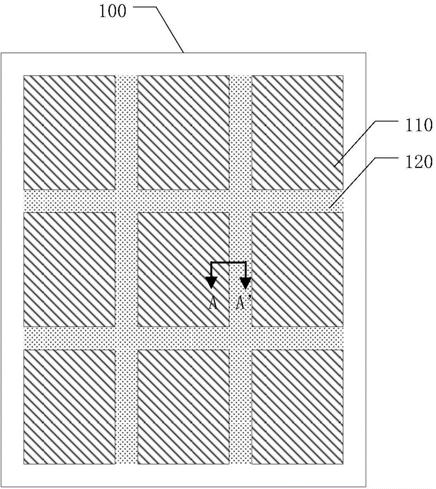
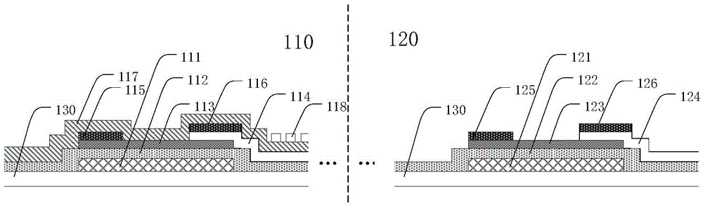
[0023] An embodiment of the present invention provides an array substrate mother board, including a plurality of display areas and a non-display area between any two adjacent display areas, the display area is provided with a first pixel unit for display, A second pixel unit is arranged on the non-display area, and the second pixel unit is used for testing the characteristics of the thin film transistor on the motherboard of the array substrate.

[0024] In the array substrate mother board provided by the embodiment of the present invention, a second pixel unit is set in the non-display area between two adjacent display areas, and the characteristics of the thin film trans...


PUM


Abstract

The invention provides an array substrate mother plate and a manufacture method thereof. The array substrate mother plate comprises a plurality of display areas and non-display areas between each two adjacent display areas, wherein first pixel units used to display are arranged on the display areas, second pixel units are arranged on the non-display units, and the second pixel units are used to test characters of thin film transistors on the array substrate mother plate. According to the array substrate mother plate, the second pixel units are arranged on the non-display units between the each two adjacent display areas, the characters of the thin film transistors on the non-display areas can be tested through the second pixel units, and therefore the characters of the thin film transistors on the display areas can be reflected, and therefore undesirable thin film transistors on the array substrate mother plate can be found timely, a plurality of following defective products can be avoided, materials can be saved, and research and development of products are facilitated.

Description

technical field [0001] The present invention relates to the display field, in particular to an array substrate motherboard and a manufacturing method thereof. Background technique [0002] TFT-LCD (Thin Film Transistor-Liquid Crystal Display Panel), as a flat panel display device, is increasingly being used in high-performance displayed in the field. [0003] Existing liquid crystal display panels mainly include an array substrate, a color filter substrate, and a liquid crystal layer. Among them, a plurality of thin film transistors (TFTs) are formed on the array substrate. However, since the thin-film transistors of the array substrate are usually covered by a protective layer, it brings a lot of inconvenience to the test of its characteristics, especially for the liquid crystal display panel in ADS mode. There is no effective method to confirm the characteristics of the TFT in the display area, so it is impossible to accurately judge whether the characteristics of the th...

Claims


Application Information

Patent Timeline
Patent Type & Authority Applications(China)
IPC IPC(8): G02F1/1362G02F1/1343
CPCG02F1/134309G02F1/1362G02F1/134318G02F1/136254G02F1/1309H01L22/34G02F1/133345G02F1/13439G02F1/1368G02F2201/121G02F2201/123G02F2201/124G02F2201/50H01L27/124H01L27/1259
Inventor 薛静尹岩岩赵龙王海金
Owner BOE TECH GRP CO LTD
Why Eureka
Try Eureka