
Trench Schottky diode terminal structure and preparation method thereof
A technology of Schottky diode and terminal structure, which is applied in semiconductor/solid-state device manufacturing, electrical components, circuits, etc., can solve problems such as device structural characteristics and unstable process methods, improve withstand voltage and reliability performance, reduce The effect of small leakage current and increased reverse withstand voltage capability
- Summary
- Abstract
- Description
- Claims
- Application Information
AI Technical Summary
Problems solved by technology
Method used
Image

Examples
specific Embodiment approach
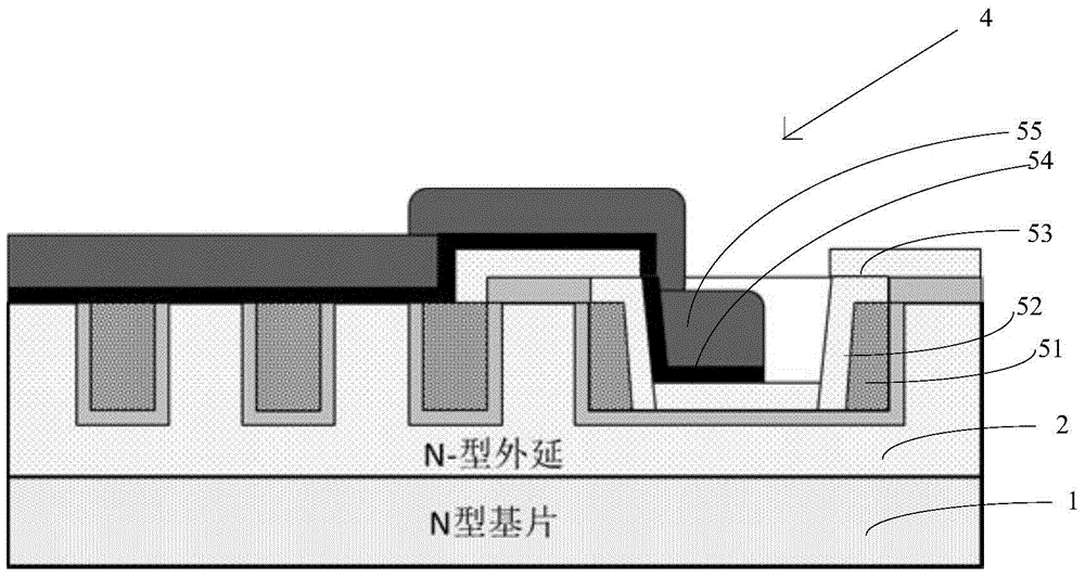
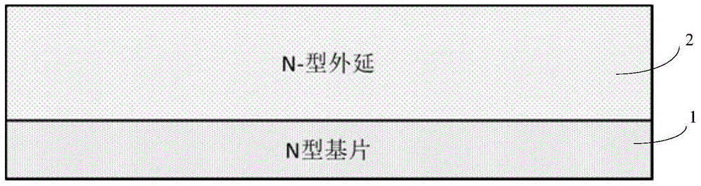
[0036] Such as figure 1 As shown, a trench Schottky diode termination structure includes an N-type silicon substrate 1, and one side of the N-type silicon substrate 1 is also provided with an N-type silicon epitaxial layer 2, and the N-type silicon epitaxial layer 1 There are several first grooves 21 inside, and a terminal ring structure 4 is arranged on one side of the first grooves 21 .
[0037] The terminal ring structure 4 of the present invention includes a second trench 22 and a third trench 23 disposed in the N-type silicon epitaxial layer, and the size of the third trench is larger than that of the first trench 21, and The size of the second groove 22 is the same as that of the first groove 21. In this embodiment, the first groove 21 and the second groove 22 are arranged at equal intervals, and the first groove 21 and the second groove 22 are small in size. groove, and the third groove 23 is a third groove.
[0038] The present invention also includes a first oxide l...
PUM
 Abstract
Description
Claims
Application Information