Optical coupling device and forming method thereof

An optical coupling device and bonding technology, which is applied in the coupling of optical waveguides, semiconductor devices, electrical components, etc., can solve the problems of unfavorable optical waveguide device performance and low coupling efficiency, and achieve the effect of preventing mutual interference and improving performance

Active Publication Date: 2015-09-09
SEMICON MFG INT (SHANGHAI) CORP +1
View PDF3 Cites 5 Cited by
  • Summary
  • Abstract
  • Description
  • Claims
  • Application Information

AI Technical Summary

Problems solved by technology

[0007] However, the coupling efficiency of the grating coupling technology in the prior art is low, which is not conducive to improving the performance of the optical waveguide device

Method used


Image

  • Optical coupling device and forming method thereof
  • Optical coupling device and forming method thereof
  • Optical coupling device and forming method thereof

Examples


Embodiment Construction

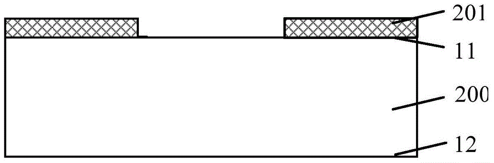
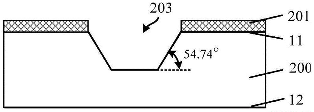
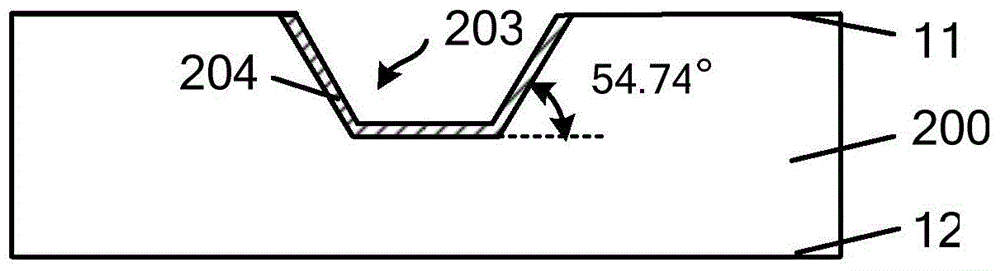
[0037] In the prior art three-dimensional packaging structure, grating coupling is usually used to realize the connection between the two planar optical waveguides on the silicon substrate. Since the grating coupling is not reflective coupling, the loss of light waves during the coupling process Larger, the coupling efficiency is very low, usually the grating coupling efficiency is only 20% to 70%.

[0038] To this end, an embodiment of the present invention provides an optical coupling device and a method for forming the same. The coupling device of the present invention includes: a first semiconductor substrate and a second semiconductor substrate. The first groove on the first surface of the bottom, the sidewall of the first groove has a first inclination angle, the sidewall and the bottom surface of the first groove have a first reflective layer; the second semiconductor substrate has A second groove penetrating the third surface of the second semiconductor substrate, the sid...


PUM


Abstract

Provided is an optical coupling device and a forming method thereof. The optical coupling device comprises a first semiconductor substrate, a first groove, a first reflecting layer, a second semiconductor substrate, a second groove, and a second reflecting layer. The first semiconductor substrate comprises a first surface and a second surface opposite to the first surface. The first groove is arranged in the first semiconductor substrate and passes through the first surface of the first semiconductor substrate. The sidewall of the first groove is provided with a first inclination angle. The first reflecting layer is arranged on the surfaces of the sidewall and the bottom of the first groove. The second semiconductor substrate comprises a third surface and a fourth surface opposite to the third surface. The second groove is arranged in the second semiconductor substrate and passes through the third surface of the second semiconductor substrate. The sidewall of the second groove is provided with a second inclination angle. The first inclination angle and the second inclination angle are mutually complementary. The second reflecting layer is arranged on the surfaces of the sidewall and the bottom of the second groove. The first surface of the first semiconductor substrate and the third surface of the second semiconductor substrate are bonded together in order that the first groove and the second groove correspond to each other. The optical coupling device improves coupling efficiency.

Description

Technical field [0001] The invention relates to the field of semiconductor manufacturing, and more particularly to an optical coupling device and a forming method thereof. Background technique [0002] Optical waveguide (optical waveguide) is a guiding structure composed of an optically transparent medium (such as quartz glass) that transmits optical frequency electromagnetic waves. The transmission principle of the optical waveguide is that on the interface of different refractive index media, the phenomenon of total reflection of electromagnetic waves causes the optical wave to propagate within the waveguide and the limited area around it. [0003] Among the many optical waveguide materials used in the communication band, the silicon-on-insulator material is easy to fabricate sub-micron-level low-loss optical waveguides due to its strong light confinement ability. At the same time, the manufacturing process is compatible with the manufacturing process of microelectronic integrate...

Claims


Application Information

Patent Timeline
Patent Type & Authority Applications(China)
IPC IPC(8): H01L31/12H01L31/18G02B6/24
CPCG02B6/24H01L31/12H01L31/18H01L31/1876Y02P70/50
Inventor 陈福成洪中山
Owner SEMICON MFG INT (SHANGHAI) CORP
Why Eureka
Try Eureka