Basic etching back-polishing process for crystalline silicon battery

A crystalline silicon battery, alkaline technology, applied in the direction of circuits, electrical components, sustainable manufacturing/processing, etc., can solve the problems of unfavorable weak light effect, high leakage ratio, damage to p-n, etc., to avoid surface defects and low leakage ratio , does not cause the effect of increasing square resistance

Inactive Publication Date: 2015-09-09
RISEN ENERGY
View PDF6 Cites 6 Cited by
  • Summary
  • Abstract
  • Description
  • Claims
  • Application Information

AI Technical Summary

Problems solved by technology

The final result is that this kind of process wastes a lot of acid liquid; see the process flow figure 2 shown
[0006] 3) Kutler type: first remove the PSG layer on the entire surface of the silicon wafer by spraying, and then edge-cutting, this process will cause the p-n junction to be exposed to acid mist during edge-cutting, thereby destroying the p-n, resulting in an increase in square resistance
The parallel resistance of batteries made by this process is generally an order of magnitude lower than that of wet etching, which is not conducive to weak light effects, and the leakage ratio is relatively high

Method used


Image

  • Basic etching back-polishing process for crystalline silicon battery
  • Basic etching back-polishing process for crystalline silicon battery
  • Basic etching back-polishing process for crystalline silicon battery

Examples


Embodiment

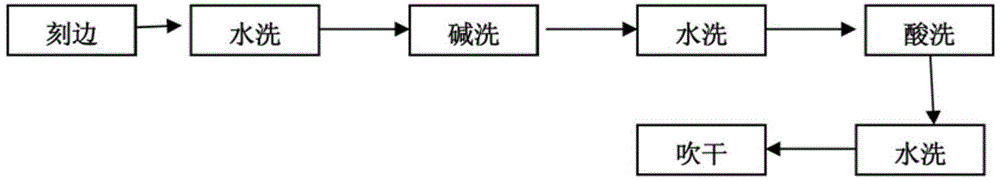
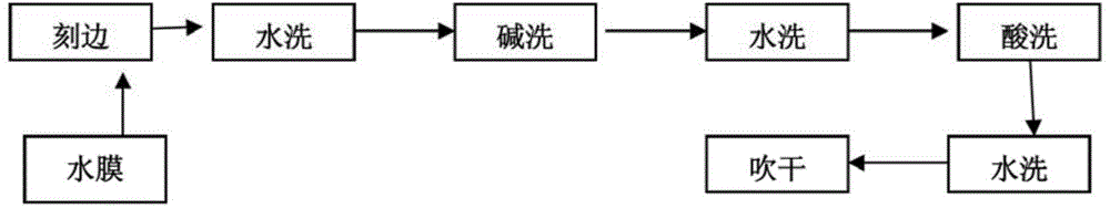
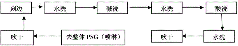
[0027] An alkaline etching back-throwing process for a crystalline silicon battery comprises the following specific steps:

[0028] 1) Use the nozzle to spray water on the front of the silicon wafer to protect the PSG layer on the front of the silicon wafer; due to the protection of the PSG layer on the front of the silicon wafer, the acid mist cannot directly corrode the P-N junction, making the square resistance stable.

[0029] 2) Use HF solution to remove the PSG layer on the back of the silicon wafer by means of capillary rollers; due to the protection of the water film, the PSG layer on the front of the silicon wafer will not be removed;

[0030] 3) Clean the residual HF solution on the silicon wafer in the water tank; prevent the HF solution from being brought into the alkali tank, and neutralize the alkali in the alkali tank;

[0031] 4) Dry the surface of the silicon wafer through a hot air knife with a temperature of 50-70°C; prevent water from being brought into the...


PUM


Abstract

The invention discloses a basic etching back-polishing process for crystalline silicon batteries. The basic etching back-polishing process includes spraying water on the front side of a silicon chip to protect the front side PSG layer of the silicon chip, removing PSG layer on the back side of the silicon chip with HF solution, washing in a water tank, drying the surface the silicon chip through blowing, transmitting the silicon chip into an immersion type alkali groove to corrode the back side of the silicon chip with weak base, washing in a water tank, removing the PSG layer on the front side of the silicon chip with HF solution, washing in a water tank, and drying by blowing. The basic etching back-polishing process ensures efficiency and stability of batteries, no etching stamps may be formed to affect the appearance of the battery, and p-n junctions may not be damaged. Acid consumption may be lowered, the back polishing effect is excellent, and no acid corrosion is on the front side. Weak photoelectric effect is facilitated, the electric leakage proportion is low, and sheet resistance may not be increased.

Description

technical field [0001] The invention relates to the field of crystalline silicon solar cells, in particular to an alkaline etching back-throwing process for crystalline silicon cells. Background technique [0002] With the release of solar profit margins for crystalline silicon cells, the competition is getting bigger and bigger. How to reduce costs and improve the yield has become one of the important issues for every enterprise. The edge engraving process is one of the most important joints of crystalline silicon cells. Various edge engraving methods are currently popular in the market, but all have their shortcomings. [0003] Mainstream etching process: [0004] 1) Rena type: The method of "floating on water" is adopted. Since the PSG layer on the surface of the silicon wafer after diffusion is hydrophilic, the acid will climb to the surface of the silicon wafer when the mixed acid is edged, and it is easy to form an "etching mark" and affect the appearance of the batte...

Claims


Application Information

Patent Timeline
Patent Type & Authority Applications(China)
IPC IPC(8): H01L31/18
CPCH01L31/18Y02P70/50
Inventor 张文锋陈波崔红星
Owner RISEN ENERGY
Why Eureka
Try Eureka