Optical device

A technology of optical devices and light-emitting layers, which is applied in lasers, electric solid-state devices, semiconductor devices, etc., can solve the problems of reduced brightness and reduced light export efficiency, and achieve the effect of improving export efficiency

Active Publication Date: 2015-09-09
DISCO CORP
View PDF7 Cites 4 Cited by
  • Summary
  • Abstract
  • Description
  • Claims
  • Application Information

AI Technical Summary

Problems solved by technology

As a result, there is a problem that the derivation efficiency of light in the optical device is lowered, and the luminance is also lowered

Method used


Image

  • Optical device
  • Optical device
  • Optical device

Examples


Embodiment Construction

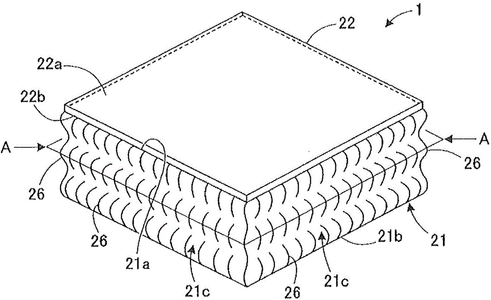
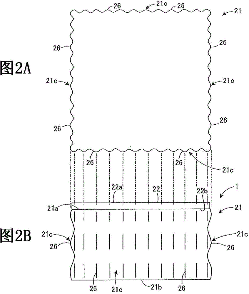
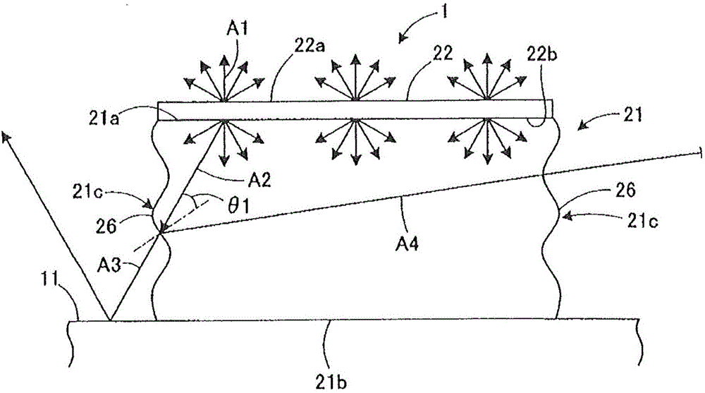
[0034] Hereinafter, the optical device of the present embodiment will be described with reference to the drawings. figure 1 It is a perspective view which shows typically the structural example of the optical device of this embodiment. Figure 2A Yes figure 1 Schematic diagram of the AA cross section of , Figure 2B is a front view schematically showing an optical device. image 3 It is a cross-sectional schematic diagram for explaining the light output state of the optical device.

[0035] like figure 1 As shown in FIG. 2 , the optical device 1 includes a substrate 21 and a light-emitting layer 22 formed on a front surface 21 a of the substrate 21 . Preferably, the substrate 21 is transparent. As the substrate 21 for crystal growth, a sapphire substrate (Al 2 O 3 substrate), gallium nitride substrate (GaN substrate), silicon carbide substrate (SiC substrate), gallium oxide substrate (Ga 2 O 3 substrate) formed substrate. like image 3 As shown, the optical device 1...


PUM


Abstract

The invention provides an optical device capable of improving light derivation efficiency. The optical device (1) of the invention has a basal plate (21) and a luminous layer (22) formed on the right side of the basal plate. The basal plate has the quadrangular right side (21a); a quadrangular back side (21b) with the same shape as the right side and parallel to the right side; and four sides (21c) connecting the right side and the back side. A plurality of projections (26) projecting outwards are formed side by side along the right side of the basal plate on each side. Bumps are alternatively formed along the thickness direction of the basal plate at each projection.

Description

technical field [0001] The present invention relates to an optical device having a light-emitting layer formed on the front surface of a substrate. Background technique [0002] In the manufacturing process of optical devices such as laser diodes (LDs) and light-emitting diodes (LEDs), for example, by epitaxial growth, a light-emitting layer (epitaxial layer) is laminated on the upper surface of a crystal growth substrate made of sapphire, SiC, or the like, thereby producing An optical device wafer for forming a plurality of optical devices is produced. Optical devices such as LDs and LEDs are formed on the front surface of the optical device wafer in each region demarcated by the planned division lines in a lattice shape. Thereby, an optical device is produced. [0003] Conventionally, the methods described in Patent Documents 1 and 2 are known as methods of dividing the optical device wafer along the lines to be divided. In the dividing method of Patent Document 1, firs...

Claims


Application Information

Patent Timeline
Patent Type & Authority Applications(China)
IPC IPC(8): H01L33/20H01L33/22
CPCH01L33/20H01L33/22H01L25/167H01S5/0207
Inventor 深谷幸太桐原直俊
Owner DISCO CORP
Why Eureka
Try Eureka