Method for measuring surface potentials on polarised devices

A technology of surface potential and equipment, which is applied in the field of potential and nanoscale potential mapping on electronic equipment, can solve the problems of inaccurate probe measurement, easy distortion of shape and contour, and the measurement device does not allow distinction, so as to achieve simple implementation and eliminate The effect of topographical illusions

Inactive Publication Date: 2015-09-09
UNIV DE REIMS CHAMPAGNE ARDENNE
View PDF5 Cites 5 Cited by
  • Summary
  • Abstract
  • Description
  • Claims
  • Application Information

AI Technical Summary

Problems solved by technology

[0016] However, the measurement setup does not allow to distinguish between actual changes in the surface topography profile and the presence of additional interaction forces due to the polarization of the sample
Therefore, the obtained topography profile is easily distorted
Therefore, the surface potential measurement of the probe is also inaccurate, since the height at which the probe is placed during the second scan is set based on the topography measurements taken in the first scan

Method used


Image

  • Method for measuring surface potentials on polarised devices
  • Method for measuring surface potentials on polarised devices
  • Method for measuring surface potentials on polarised devices

Examples


example 1

[0071] Example 1 : Demonstration of the method according to the invention on a polarized electronic device of the OFET type

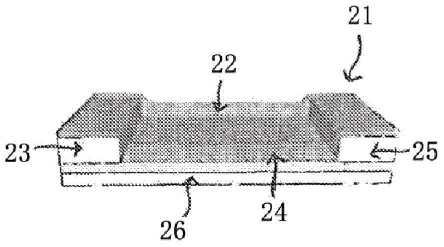
[0072] The method has been implemented on polarized electronic devices, more specifically on OFET transistors (Organic Field Effect Transistors) 21, such as Figure 3A As shown, and wherein the semiconductor material 22 is composed of poly(3-hexylthiophene) or P3HT deposited on the electrode structure forming the transistor.

[0073] In particular, transistors of this type can withstand applied voltages up to ±100 V, which can cause problems when measuring their topographical profiles.

[0074] The OFET transistor 21 comprises three regions, namely 23 , 24 and 25 , which are associated.

[0075] More specifically, region 23 corresponds to a potentiostatic "drain" electrode, intermediate region 24 corresponds to the channel of transistor 21, and region 25 corresponds to a potentiostatic "source" electrode.

[0076] Polarization of transistor 21 is ex...


PUM


Abstract

A method for measuring the surface potential of a polarized sample includes: measuring the topographic profile of the sample by scanning its surface with a tapered tip connected to a micro-lever activated at the resonance frequency of same by a piezoelectric actuator; placing the tapered tip a constant distance away from the topographic profile of the surface obtained during the previous step; and measuring the electrostatic potential of the surface. The sample is not polarized during the step of measuring the topographic profile. The sample is polarized during the measurement of the potential profile.

Description

technical field [0001] The invention relates to the field of polarized electronics. [0002] In particular, the invention relates to a method of measuring the potential on an electronic device polarized by an external voltage source. [0003] More specifically, the method of the present invention enables nanoscale potential mapping that can be applied to semiconductor devices. Background technique [0004] According to the state of the art, it is currently known to use atomic force microscopy (or AFM for "atomic force microscopy") in order to visualize the topography of the surface of a sample (eg polarized electronic devices such as semiconductor devices). [0005] An atomic force microscope is a scanning probe microscope in which the probe is in the form of a tapered tip. This microscope is capable of analyzing regions with scales ranging from a few nanometers to a few micrometers, and measuring forces in the nano-Newton range. [0006] The probe of an AFM microscope is...

Claims


Application Information

Patent Timeline
Patent Type & Authority Applications(China)
IPC IPC(8): G01Q60/30
CPCG01Q30/20G01B11/30G01Q60/30B82Y35/00
Inventor 路易·吉罗德尼古拉·波格丹·贝库奥利佛·西摩内提让-路易·尼古拉斯米歇尔·莫里那利
Owner UNIV DE REIMS CHAMPAGNE ARDENNE
Why Eureka
Try Eureka