Touch control display substrate

A technology of touch display substrate and touch scanning, which is applied in the direction of static indicators, optics, instruments, etc., can solve the problems of reducing accuracy and setting time difference of touch effect detection, so as to reduce the difference and improve the accuracy , the effect of difference reduction

Active Publication Date: 2015-09-23
XIAMEN TIANMA MICRO ELECTRONICS +1
View PDF5 Cites 17 Cited by
  • Summary
  • Abstract
  • Description
  • Claims
  • Application Information

AI Technical Summary

Problems solved by technology

The difference in parasitic capacitance will lead to differences in the setting time of touch effect detection corresponding to each common electrode block
However, for the detection of the ...

Method used


Image

  • Touch control display substrate
  • Touch control display substrate
  • Touch control display substrate

Examples


Embodiment 1

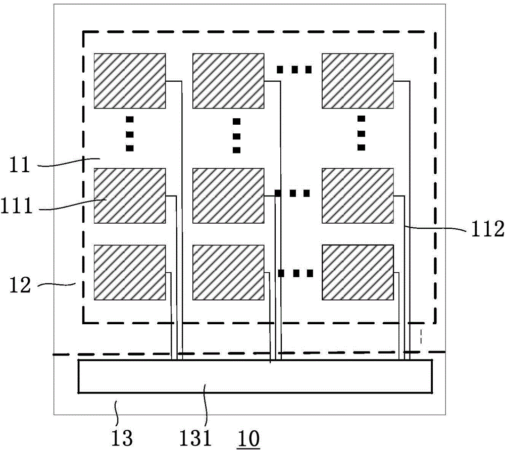
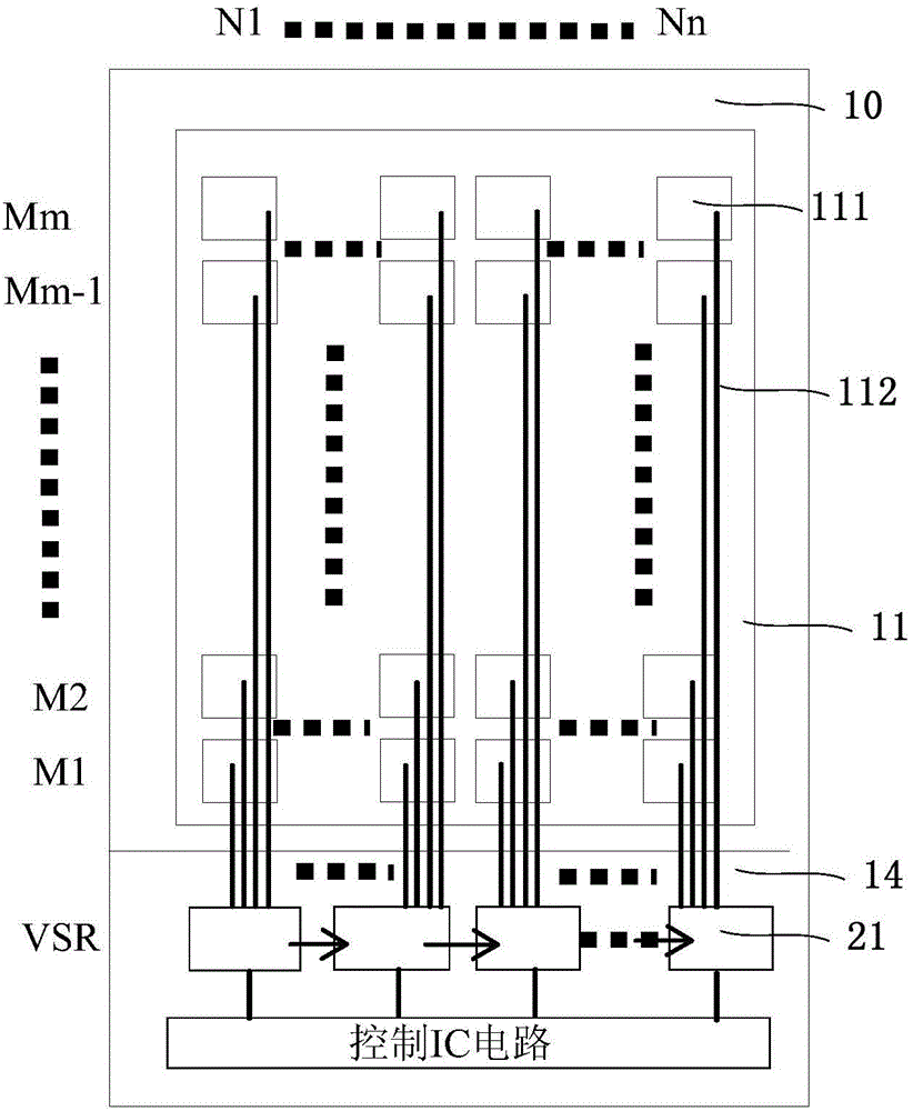
[0043] Embodiment 1 of the present invention provides a touch display substrate. figure 2 It is a structural diagram of the touch display substrate provided by Embodiment 1 of the present invention.

[0044] Such as figure 2 As shown, the touch display substrate includes:

[0045] A substrate 10, including a display area 11 and a non-display area 14;

[0046] A plurality of common electrode blocks 111 arranged at intervals, the common electrode blocks 111 form an array of M rows*N columns, and the common electrode blocks 111 are multiplexed as touch electrodes;

[0047] A plurality of wires 112, each wire 112 is electrically connected to a common electrode block 111;

[0048]A vertical shift circuit, arranged in the non-display area 14 and electrically connected to the wiring 112, the vertical shift circuit includes a plurality of cascaded vertical shift circuit units 21, each vertical shift circuit unit 21 is connected to the wiring 112 corresponding to a column of comm...

Embodiment 2

[0064] Embodiment 2 of the present invention provides a touch display substrate. The touch display substrate divides the common electrode block into two symmetrical common electrode block groups according to the column direction, and the control IC circuit is used to apply different frequencies to different common electrode block groups in different touch scanning time periods. scan pulse signal. Figure 6 and Figure 7 They are respectively the first state diagram and the second state diagram of different common electrode block groups applying scan pulse signals with different frequencies provided by Embodiment 2 of the present invention.

[0065] Such as Figure 6 and Figure 7 As shown, on the basis of the first embodiment, this embodiment divides the common electrode block into two symmetrical common electrode block groups in the column direction.

[0066] The control IC circuit is used to apply a scanning pulse signal of a first frequency to the first common electrode...

Embodiment 3

[0072] Embodiment 3 of the present invention provides a touch display substrate. The touch display substrate divides the common electrode block into three common electrode block groups in the column direction, and the control IC circuit is used to apply to different common electrode block groups in different touch scanning time periods. Scanning pulse signals with different frequencies. Figure 9 , Figure 10 and Figure 11 They are respectively the first state diagram, the second state diagram and the third state diagram of applying scanning pulse signals with different frequencies to different common electrode block groups provided by Embodiment 3 of the present invention.

[0073] Such as Figure 9 , Figure 10 and Figure 11 As shown, on the basis of the first embodiment, this embodiment divides the common electrode block into three common electrode block groups divided into three equal parts in the column direction.

[0074] The control IC circuit is used to apply a...


PUM


Abstract

The invention relates to a touch control display substrate, comprising a substrate, a plurality of common electrode blocks arranged at interval, a plurality of wires, a vertical shift circuit, and a control IC circuit. The vertical shift circuit comprises a plurality of vertical shift circuit units in cascade connection. Each vertical shift circuit unit is connected with the wires corresponding to a row of the common electrode blocks. The vertical shift circuit unit is used to output touch control drive signals to corresponding row of common electrode blocks in sequence. The control IC circuit is used to output touch control drive signals to the vertical shift circuit. The common electrode blocks are divided into n common electrode block groups according to row directions. The control IC circuit is used to apply scanning pulse signals in different frequency to different common electrode block groups in different touch control scanning time periods, so as to compensate different load cased by different distances between different common electrode blocks and the control IC circuit, and improve accuracy of touch control effect detection of different common electrode blocks.

Description

technical field [0001] The present invention relates to the technical field of liquid crystal display, in particular to a touch display substrate. Background technique [0002] In the existing in-cell touch panel (In Cell Touch Panel), the common electrode layer of the liquid crystal display panel (Liquid Crystal Display, LCD) is generally divided into a plurality of common electrode blocks, and each common electrode block is respectively passed through a wiring It is electrically connected with a control IC (integrated circuit). The common electrode blocks are multiplexed as touch electrodes. In the display state, the common electrode block is used to receive a common voltage signal, and in the touch state, the common electrode block is used as a touch driving electrode and used to receive a touch driving signal. [0003] Generally, the traces connected to the common electrode block will couple with other traces of the display to generate parasitic capacitance, and as the...

Claims


Application Information

Patent Timeline
IPC IPC(8): G02F1/1333G02F1/1343G09G3/36
CPCG02F1/13338G02F1/134309G09G3/36G06F3/0412G06F3/04166G06F3/0443G06F2203/04103
Inventor 胡盛棚杨毅志黄建才许育民
Owner XIAMEN TIANMA MICRO ELECTRONICS
Why Eureka
Try Eureka