Junction termination structure of thyristor chip

A thyristor and junction terminal technology, which is applied in the field of chip junction terminal structure, can solve the problems of forward and reverse voltage asymmetry and low withstand voltage, and achieve the effects of increasing surface area, improving stability and reducing surface electric field intensity

Active Publication Date: 2015-09-23
ANHUI PROVINCE QIMEN COUNTY HUANGSHAN ELECTRIC APPLIANCE
View PDF5 Cites 5 Cited by
  • Summary
  • Abstract
  • Description
  • Claims
  • Application Information

AI Technical Summary

Problems solved by technology

[0003] The purpose of the present invention is to provide a junction terminal structure of a thyristor chip to solve the problems of low withstand voltage and serious asymmetry of forward and reverse voltages of the junction terminal structure of the existing thyristor chip

Method used


Image

  • Junction termination structure of thyristor chip
  • Junction termination structure of thyristor chip
  • Junction termination structure of thyristor chip

Examples


Embodiment 1

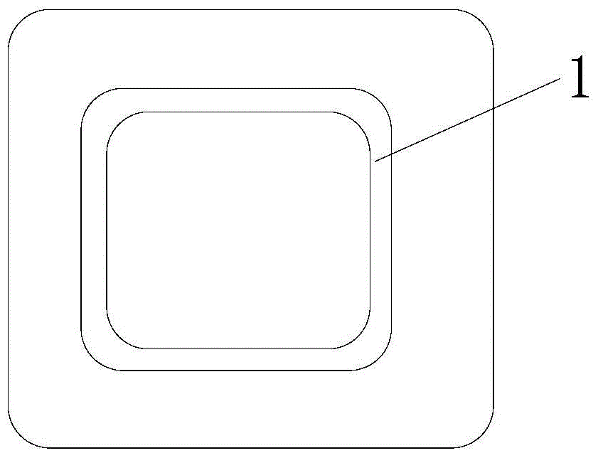
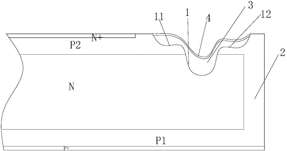
[0012] Embodiment 1: A junction terminal structure of a thyristor chip, such as figure 1 , figure 2 As shown, it includes long base area N, short base area P1, P2, isolation wall 2, phosphorus diffusion area N+, boron-concentrated diffusion area P+, voltage groove 1, and the voltage groove 1 is in a ring structure; the voltage groove 1 is a voltage tank structure with high voltage resistance and weak surface electric field. The depth of the voltage tank 1 is over P 2 The N junction extends into the long base region N20-70um. The inner surface of the voltage tank 1 is provided with an insulating layer 3 , and a glass passivation layer 4 is provided on the insulating layer. Take the designed thyristor chip with a peak theoretical withstand voltage of 2400V as an example:

[0013] When the traditional voltage tank structure is adopted, the peak withstand voltage is 1400V; when the one-step structure is adopted, the peak withstand voltage can reach 1900-2200V. The specific p...

Embodiment 2

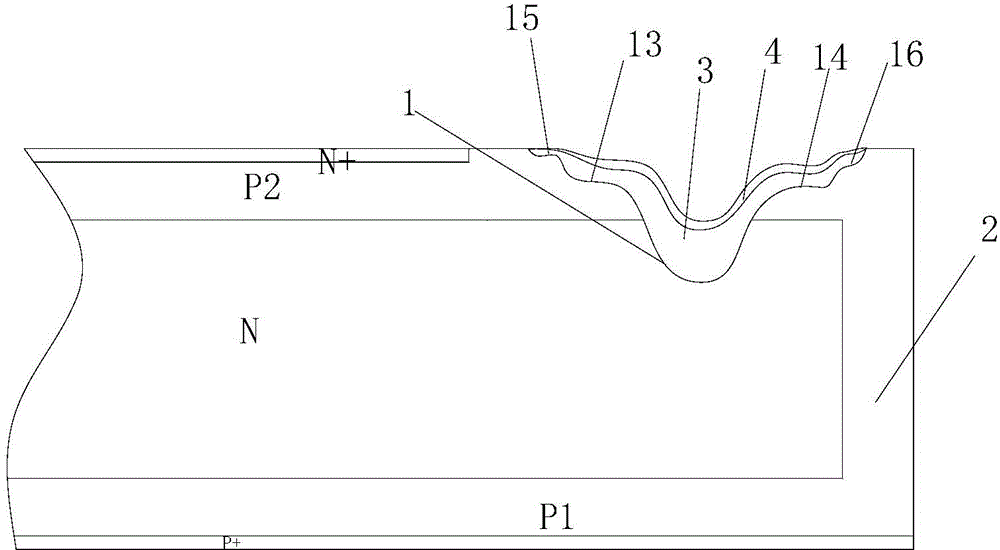
[0018] A junction termination structure of a thyristor chip, such as figure 1 , image 3 As shown, it includes long base area N, short base area P1, P2, isolation wall 2, phosphorus diffusion area N+, boron-concentrated diffusion area P+, voltage groove 1, and the voltage groove 1 is in a ring structure; the voltage groove 1 is a voltage tank structure with high voltage resistance and weak surface electric field. The depth of the voltage tank 1 is over P 2 The N junction extends into the long base region N20-70um. An insulating layer 3 is arranged on the inner surface of the voltage tank 1 , and a glass passivation layer 4 is arranged on the insulating layer 3 . Take the designed thyristor chip with a theoretical withstand voltage peak value of 3500V as an example:

[0019] When the traditional voltage tank structure is adopted, the peak withstand voltage is best at 1800V; when the one-level stepped structure is adopted, the peak withstand voltage is optimally 2800V, and w...


PUM


Abstract

The present invention discloses a junction termination structure of a thyristor chip, and the problems of low forward voltage withstand value and large leakage current of a chip in an existing thyristor single-face trench are solved. Two inner walls of the voltage groove in the thyristor single-face trench are symmetrically provided with stepped structures. The voltage trench is provided with two-stage stepped structures or three-stage stepped structures, the height is larger than a P2N junction, and the structures extend into an N area for 20um to 70 um. The junction termination structure is suitable for the semiconductor chip production field of all table top structures.

Description

technical field [0001] The invention relates to a chip junction terminal structure of a power semiconductor device, in particular to a junction terminal structure of a thyristor chip. Background technique [0002] In the manufacturing process of the thyristor chip, in order to form a good withstand voltage, it is usually realized by digging grooves on the table and adding insulating layer protection. The existing single-groove process forms a bell mouth structure with a shape of 70-90 degrees after the groove is excavated. This structure bears a relatively low withstand voltage, usually with a peak voltage of 600-1400V. At the same time, the structure can withstand forward and reverse The voltage is asymmetrical, and the reverse withstand voltage is higher than the forward withstand voltage. The reason is that this structure causes the space charge region to not expand widely, and the electric field is concentrated, resulting in low forward withstand voltage, and the revers...

Claims


Application Information

Patent Timeline
Patent Type & Authority Applications(China)
IPC IPC(8): H01L29/06
CPCH01L29/0607H01L29/74
Inventor 王民安黄富强项建辉叶民强汪杏娟王日新
Owner ANHUI PROVINCE QIMEN COUNTY HUANGSHAN ELECTRIC APPLIANCE
Why Eureka
Try Eureka