An optically transparent frequency selective surface structure and its manufacturing method
A frequency selective surface, optically transparent technology, applied in the field of optical windows, can solve the problems of reducing light transmission performance, uneven energy distribution of high-order diffraction, uneven energy distribution, etc., and achieve the effect of improving light transmission performance
- Summary
- Abstract
- Description
- Claims
- Application Information
AI Technical Summary
Problems solved by technology
Method used
Image
Examples
specific Embodiment 1
[0052] This embodiment is an embodiment of an optically transparent frequency selective surface structure.
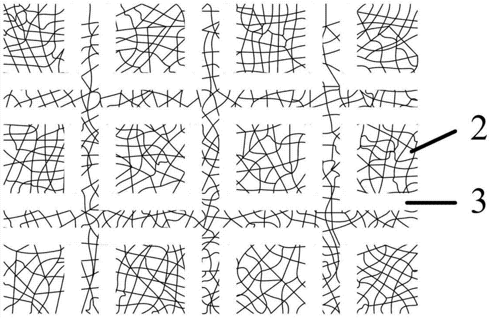
[0053] The optically transparent frequency selective surface structure of this embodiment includes a substrate 1, a transparent grid film 2 distributed on the substrate 1, and the surface of the transparent grid film 2 has a periodic opening array 3;
[0054] The shape of the transparent grid film 2 is a pattern formed by natural drying of cracked nail polish containing acrylic resin under the temperature of 20-25°C and humidity of 50-80%RH;
[0055] The inside of the periodic hole array 3 has one of the following two structures:
[0056] Structure 1, does not contain transparent grid film 2;
[0057] The second structure contains a transparent grid film 2, and the transparent grid film 2 inside the hole is not connected to the transparent grid film 2 outside the hole.
[0058] Here, the periodic hole array 3 is a square ring, the periodic hole array 3 contains a tran...
specific Embodiment 2
[0060] This embodiment is still an optically transparent frequency selective surface structure embodiment.
[0061] The optically transparent frequency selective surface structure of this embodiment includes a substrate 1, a transparent grid film 2 and a periodic hole array 3 distributed on the substrate 1; the transparent grid film 2 and the periodic hole array 3 are specifically The exchange of corresponding positions described in Embodiment 1.
specific Embodiment 3
[0063] This embodiment is an embodiment of a method for fabricating an optically transparent frequency selective surface structure.
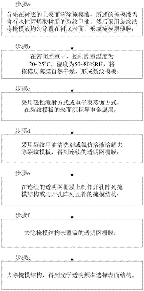
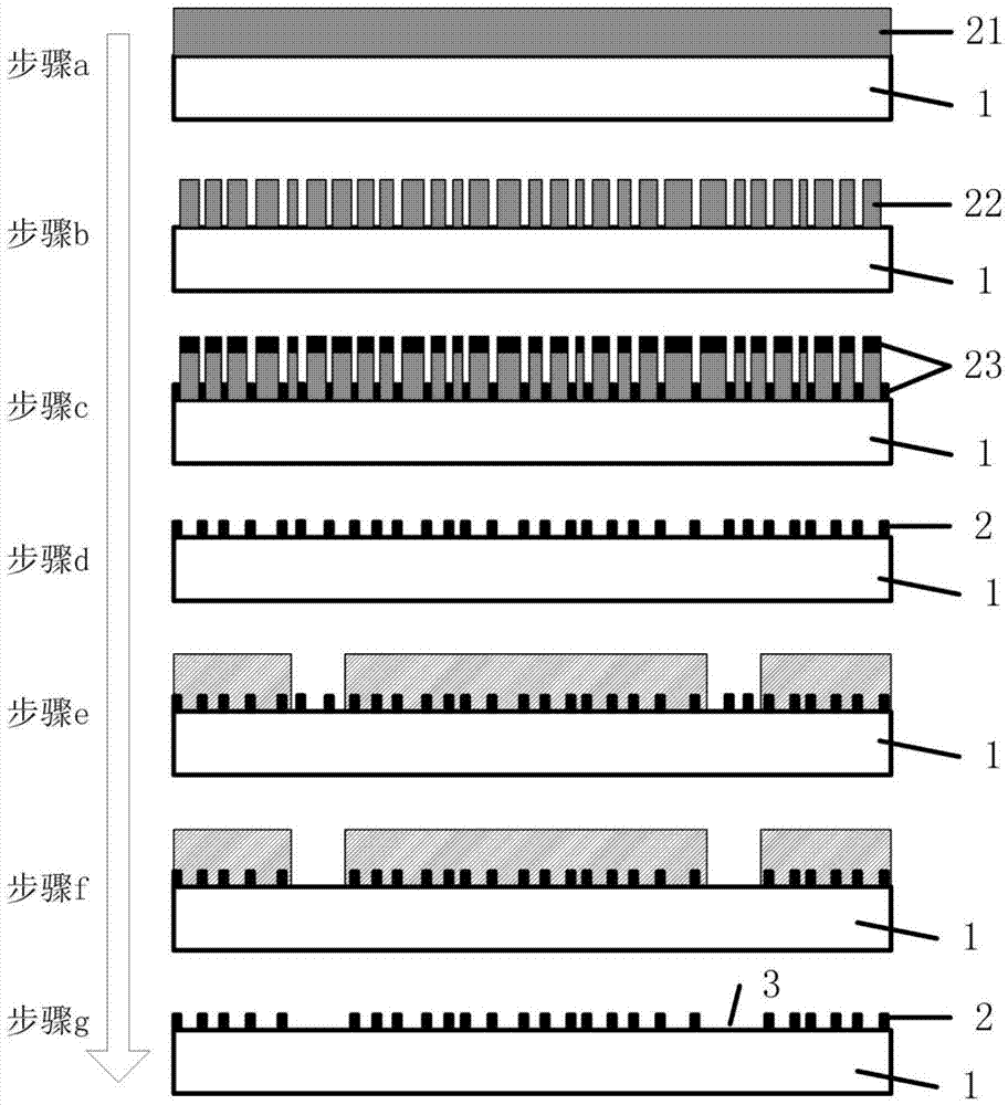
[0064] The manufacturing method of the optically transparent frequency selective surface structure of the present embodiment, the flow chart is as follows figure 2 shown. The method includes the following steps:
[0065] In step a, first drop-coat a masking liquid on the upper surface of the substrate 1, the masking liquid is cracked nail polish containing water-based acrylic resin, and then uniformly coat the masking liquid on the surface of the substrate 1 by a spin coating method , forming a mask layer film 21;
[0066] Step b, in a closed chamber, control the temperature of the chamber to 20-25° C. and the humidity to 50-80% RH, and dry the mask layer film 21 naturally to form the crack template 22;
[0067] Step c, using magnetron sputtering or electron beam evaporation to deposit a conductive metal layer 23 on the surface of the cracke...
PUM
 Abstract
Description
Claims
Application Information


