An electrochromic glass
An electrochromic glass, glass plate technology, applied in nonlinear optics, instruments, optics, etc., can solve the problems of affecting the light transmission performance and electrical conductivity of glass, crack warping, complicated removal process, etc., to solve the light transmission performance. and the effect of reducing electrical conductivity
- Summary
- Abstract
- Description
- Claims
- Application Information
AI Technical Summary
Problems solved by technology
Method used
Image
Examples
specific Embodiment 2
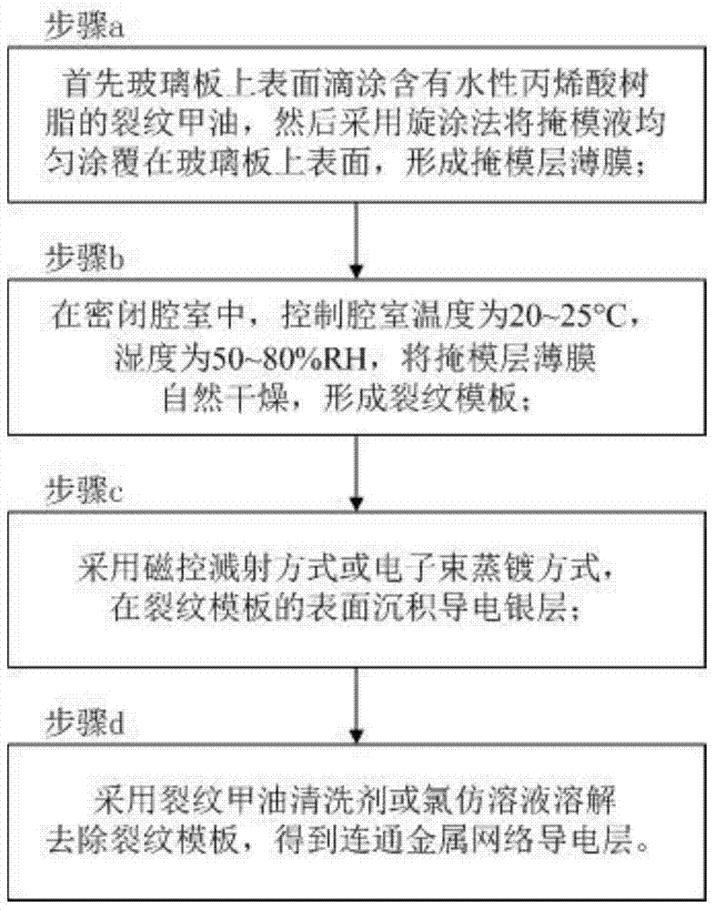
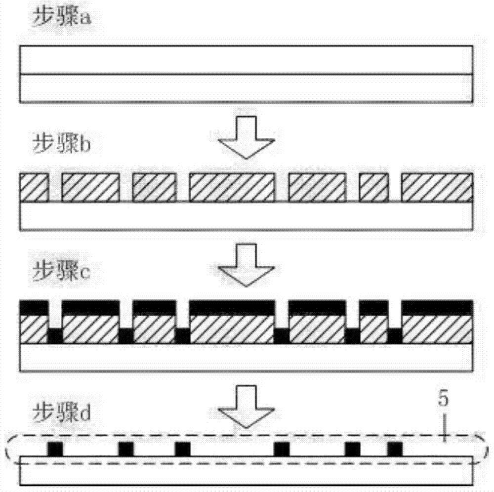
[0042] The electrochromic glass of the present embodiment, on the basis of the specific embodiment 1, further defines that the conductive layer 5 of the connected metal network adopts such as figure 2 Made by the method shown. The method is a lift-off process, comprising the following steps:
[0043] In step a, the surface of the glass plate is first drop-coated with cracked nail polish containing water-based acrylic resin, and then the masking liquid is evenly coated on the surface of the glass plate by a spin coating method to form a mask layer film;
[0044] Step b, in a closed chamber, the temperature of the chamber is controlled to be 20-25° C., the humidity is 50-80% RH, and the mask layer film is naturally dried to form a crack template;
[0045] Step c, using magnetron sputtering or electron beam evaporation to deposit a conductive silver layer on the surface of the cracked template;
[0046] In step d, the cracked nail polish cleaning agent or chloroform solution i...
specific Embodiment 3
[0049] The electrochromic glass of this embodiment, on the basis of the specific embodiment 2, further defines the lift-off process,
[0050] The cracked nail polish described in step a is diluted with a diluent, and the dilution ratio k is defined as the volume ratio of the diluent to the cracked nail polish, and 1≤k≤7.
[0051] Under the above ratio conditions, it is found that the relationship between the average crack width w of the crack template and the film thickness h of the mask layer is:
[0052] w=0.342e 0.266h
[0053] In the formula, w is the average crack width of the crack template, in μm; h is the film thickness of the mask layer, in μm.
[0054] The relationship between the average crack spacing d of the crack template and the film thickness h of the mask layer is:
[0055] d=15.8e 0.169h
[0056] In the formula, d is the average crack spacing of the crack template, in μm; h is the film thickness of the mask layer, in μm.
[0057] These two formulas show...
PUM
 Abstract
Description
Claims
Application Information


