Manufacturing method of image sensor using deep trench isolation

An image sensor and deep trench isolation technology, applied in the field of image sensors, can solve the problems affecting the quality of epitaxial single crystal silicon, dislocation or void defects, etc., and achieve the effect of good shape, not easy to dislocation and void, and excellent interface

Inactive Publication Date: 2015-09-30
GALAXYCORE SHANGHAI
View PDF6 Cites 6 Cited by
  • Summary
  • Abstract
  • Description
  • Claims
  • Application Information

AI Technical Summary

Problems solved by technology

However, in the actual manufacturing process, since the width of the isolation structure is usually large (about 100-300nm), when the epitaxial single crystal silicon layers grown from the substrate surfaces on both sides of the isolation structure meet at the top of the isolation structure, It is easy to generate dislocations or void defects at the bonding site, thus affecting the quality of epitaxial single crystal silicon

Method used


Image

  • Manufacturing method of image sensor using deep trench isolation
  • Manufacturing method of image sensor using deep trench isolation
  • Manufacturing method of image sensor using deep trench isolation

Examples


Embodiment Construction

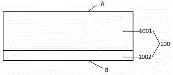
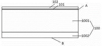
[0019] In the production process of the existing image sensor, an isolation structure composed of a dielectric layer is first formed on the substrate, and then an epitaxial monocrystalline silicon layer covering the isolation structure is formed by selective epitaxy. Since the width of the isolation structure is usually large ( about 100-300nm), when the epitaxial monocrystalline silicon layers grown from the substrate surfaces on both sides of the isolation structure meet at the top of the isolation structure, it is easy to generate dislocations or void defects at the junction, thereby affecting the epitaxial monocrystalline silicon the quality of.

[0020] Therefore, the present invention proposes a method for making an image sensor using deep trench isolation. Before forming an image sensor device, a single crystal silicon wall covered with a dielectric layer is formed on the top surface and side surface as an isolation structure. The surface shape of the isolation structure...


PUM


Abstract

The invention provides a manufacturing method of image sensor using deep trench isolation. The manufacturing method includes: providing a substrate which comprises a substrate monocrystalline layer; etching the substrate monocrystalline layer to form a plurality of monocrystalline walls raised, the top and lateral surfaces of each which are covered with a dielectric layer; subjecting the surface of the substrate monocrystalline layer between the monocrystalline walls to selective epitaxy so as to form a first epitaxial monocrystalline layer, removing the part, covering the top surfaces of the monocrystalline walls, of the dielectric layer so as to expose the top surfaces of the monocrystalline walls, and subjecting the top surfaces of the monocrystalline walls and the surface of the first epitaxial monocrystalline layer to selective epitaxy so as to form a second epitaxial monocrystalline layer; forming part of components of the image sensor in the first and second epitaxial monocrystalline layers. The manufacturing method has the advantages that the defects of the isolation structure of the epitaxial monocrystalline layers are effectively decreased, functional damage to the components of the image sensor is avoided, and quality of the components of the image sensor is improved.

Description

technical field [0001] The invention relates to the field of image sensors, in particular to a method for manufacturing an image sensor using deep trench isolation. Background technique [0002] Image sensors can be classified into complementary metal oxide (CMOS) image sensors and charge-coupled device (CCD) image sensors. The advantage of the CCD image sensor is that it has high image sensitivity and low noise, but it is difficult to integrate the CCD image sensor with other devices, and the power consumption of the CCD image sensor is relatively high. In contrast, CMOS image sensors have the advantages of simple process, easy integration with other devices, small size, light weight, low power consumption, and low cost. Therefore, with the development of technology, CMOS image sensors are increasingly used in various electronic products instead of CCD image sensors. At present, CMOS image sensors have been widely used in still digital cameras, camera phones, digital vide...

Claims


Application Information

Patent Timeline
Patent Type & Authority Applications(China)
IPC IPC(8): H01L27/146H01L21/762
Inventor 赵立新杨瑞坤
Owner GALAXYCORE SHANGHAI
Why Eureka
Try Eureka