
Circuit board tin spraying process

A circuit board and process technology, which is applied in the field of circuit board tin spraying process, can solve the problems of affecting appearance, abnormal product quality, oil leakage, etc.

Inactive Publication Date: 2015-09-30
ANHUI DASHENG ELECTRONICS
View PDF3 Cites 6 Cited by
  • Summary
  • Abstract
  • Description
  • Claims
  • Application Information

AI Technical Summary

Problems solved by technology

[0002] At present, the application technology of circuit boards has been greatly developed with the development of electronic technology, and users have put forward higher requirements for circuit boards. Difficult to withstand high temperature, resulting in expansion, the hole wall is relatively smooth, easy to cause the plugging ink to peel off the hole wall, the plugging ink expands due to high temperature and pushes out, resulting in overflow at the edge of the hole, causing serious oil leakage, making the product The quality is abnormal and affects the appearance

Method used


Image

  • Circuit board tin spraying process

Examples


Embodiment Construction

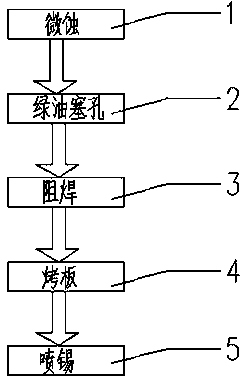
[0008] Such as figure 1 As shown, a circuit board tin spraying process, which includes micro-etching 1, green oil plug hole 2, solder mask 3, baking plate 4 and tin spraying 5 steps, the micro-etching 1 acts on the hole wall and the board surface. Form a microscopically rough surface; the green oil plug hole 2 is a double-sided plug hole, which effectively avoids the appearance of tin beads; the solder mask 3 forms a layer of ink protective layer on the surface of the circuit board; the baking plate 4 uses a temperature The step-by-step baking method of gradually increasing the temperature from 60°C to 150°C, the ink in the hole of the circuit board is not directly subjected to high temperature, but is gradually increased from low temperature to high temperature, so that the water-based solvent of the ink in the hole is completely volatilized, and the ink Slowly solidify in the hole, and the cured ink will not overflow on the edge of the hole; the time interval between the HAS...


PUM


Abstract

The invention discloses a circuit board tin spraying process, which comprises the steps of microetching, green oil hole plugging, welding resisting, board baking and tin spraying, wherein the microetching acts on the hole wall and the plate surface; the green oil hole plugging is double-side hole plugging; during the welding resisting, a layer of ink protecting layer is formed on the surface of a circuit board; the board baking adopts a segmented board baking method adopting sequential progressive temperature increase from 60 DEG C to 150 DEG C; the time interval between the tin spraying and the board baking is within 10 minutes. The tin spraying process has the advantages that deoiling phenomenon cannot occur, and meanwhile, the insulation, anti-oxidation and attractive appearance effects are also achieved.

Description

technical field [0001] The invention relates to the field of circuit board production, in particular to a circuit board tin spraying process. Background technique [0002] At present, the application technology of circuit boards has been greatly developed with the development of electronic technology, and users have put forward higher requirements for circuit boards. Difficult to withstand high temperature, resulting in expansion, the hole wall is relatively smooth, easy to cause the plugging ink to peel off the hole wall, the plugging ink expands due to high temperature and pushes out, resulting in overflow on the edge of the hole, serious oil leakage occurs, making the product The quality is abnormal and affects the appearance. Contents of the invention [0003] In order to overcome the above-mentioned defects in the prior art, the object of the present invention is to provide a tin-spraying process for circuit boards. [0004] The present invention is realized by adop...

Claims


Application Information

Patent Timeline
Patent Type & Authority Applications(China)
IPC IPC(8): H05K3/40H05K3/24
CPCH05K3/0094H05K3/24H05K2203/1105
Inventor 陈国康
Owner ANHUI DASHENG ELECTRONICS
Learn More