Static timing analysis method for thermal stress circuit with silicon through holes

A static timing analysis, through-silicon via technology, applied in the field of microelectronics, can solve problems such as inapplicability to circuits containing multiple types of through-silicon vias, reduced accuracy of carrier mobility changes, and reduced accuracy of thermal stress.

Active Publication Date: 2015-10-07
XIDIAN UNIV
View PDF3 Cites 4 Cited by
  • Summary
  • Abstract
  • Description
  • Claims
  • Application Information

AI Technical Summary

Problems solved by technology

[0004] Krit Athikulwonge. Jae-Seok Yang. David Z Pan. Sung Kyu Lim. "Impact of Mechanical Stress on the Full Chip Timing for Through-Silicon-Via-based 3-D ICs". IEEE Transactions on Computer-Aided Design of Integrated Circuits and Systems, VOL.32, NO.6, JUNE 2013, this paper discloses an analysis method that considers the influence of TSV thermal stress on the timing of three-dimensional integrated circuits, but the stress model used in the article is simple uniaxial stress, The influence of other layer materials is not considered, which will reduce the accuracy of thermal stress acquisition; and this method only considers cylindrical TSVs and does not consider other types of TSVs, so this method is not suitable for At the same time, the influence of the direction of the device channel is not taken into account, which will cause the accuracy of the carrier mobility change to decrease when the device channel in the circuit is along different crystal directions. , making timing analysis of the circuit unreliable

Method used


Image

  • Static timing analysis method for thermal stress circuit with silicon through holes
  • Static timing analysis method for thermal stress circuit with silicon through holes
  • Static timing analysis method for thermal stress circuit with silicon through holes

Examples


Embodiment Construction

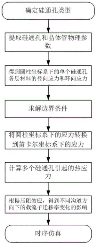
[0083] Specific embodiments of the present invention will be described in detail below.

[0084] Such as figure 1 As shown, the static timing analysis method for circuits with thermal stress through silicon vias includes the following steps:

[0085] (1) Determine the type of TSV used in the circuit;

[0086] (2) According to the type of TSV, extract the material of each layer of the TSV used and the physical parameters of the transistor from the circuit;

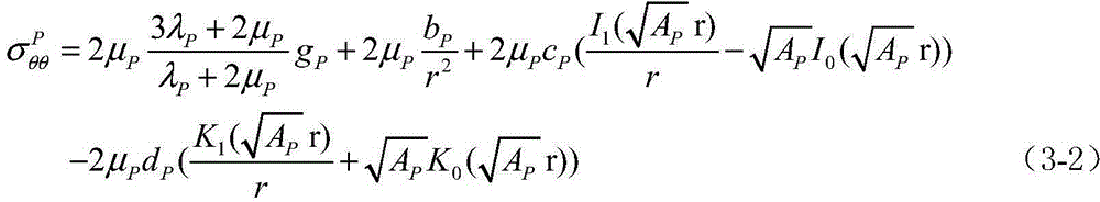
[0087] (3) According to the physical parameters of each layer material of TSV, the radial stress of each layer material of a single TSV in the cylindrical coordinate system is obtained by using the mathematical model of stress and hoop stress

[0088] σ r r P = 2 μ P 3 λ P + 2 ...


PUM


Abstract

he invention belongs to a static timing analysis method for a thermal stress circuit with silicon through holes. The method comprises the following steps of: (1) determining the types of the silicon through holes used in a circuit; (2) extracting the physical parameters of all layers of materials and transistors in the silicon through holes in the circuit; (3) obtaining the radial stress and hoop stress of all layers of materials of single silicon through hole in a cylindrical-coordinate system; (4) solving the boundary conditions of all coefficients in a stress expression; (5) converting the stress under the cylindrical-coordinate system into the stress under a cartesian coordinate system; (6) obtaining total thermal stress distribution caused by a plurality of silicon through holes according to a linear superposition norm; (7) calculating the influence on the change of carrier mobility in different channel directions; and (8) adding the change of carrier mobility to a Gate-level netlist of the circuit, and operating PrimeTime to carry out the static timing analysis under a timing constraint condition, so as to obtain the conditions of longest path time delay and timing sequence allowance change of the circuit.

Description

technical field [0001] The invention belongs to the technical field of microelectronics, and in particular relates to a static timing analysis method for thermal stress circuits with through-silicon holes. Background technique [0002] When studying the thermomechanical reliability of TSV-based 3D integrated circuits, the key is the acquisition of thermal stress. The acquisition of thermal stress is obtained through finite element analysis software and mathematical modeling. Among them, the finite element analysis is solved by dividing the finite element model of the through-silicon via, and the solution speed is slow, especially in the large-scale three-dimensional integrated circuit design, the finite element model is very complicated, which consumes a lot of time and storage resources. The mathematical modeling of the thermal stress can quickly obtain the thermal stress of the through-silicon via, so that the thermal-mechanical reliability of the through-silicon via can ...

Claims


Application Information

Patent Timeline
Patent Type & Authority Applications(China)
IPC IPC(8): G06F17/50
Inventor 董刚刘荡杨银堂
Owner XIDIAN UNIV
Why Eureka
Try Eureka