Thin film transistor and preparation method thereof, array substrate, display device

A thin-film transistor and control layer technology, which is applied in the direction of transistors, semiconductor/solid-state device manufacturing, and electric solid-state devices, can solve the problems of poor stability of thin-film transistors, improve stability, reduce threshold voltage offset, and reduce defective rate effect

Active Publication Date: 2018-02-02
BOE TECH GRP CO LTD
View PDF4 Cites 0 Cited by
  • Summary
  • Abstract
  • Description
  • Claims
  • Application Information

AI Technical Summary

Problems solved by technology

[0005] In order to solve the problem of poor stability of existing thin film transistors under light conditions, an embodiment of the present invention provides a thin film transistor and its preparation method, an array substrate, and a display device

Method used


Image

  • Thin film transistor and preparation method thereof, array substrate, display device
  • Thin film transistor and preparation method thereof, array substrate, display device
  • Thin film transistor and preparation method thereof, array substrate, display device

Examples


Embodiment Construction

[0061] In order to make the object, technical solution and advantages of the present invention clearer, the implementation manner of the present invention will be further described in detail below in conjunction with the accompanying drawings.

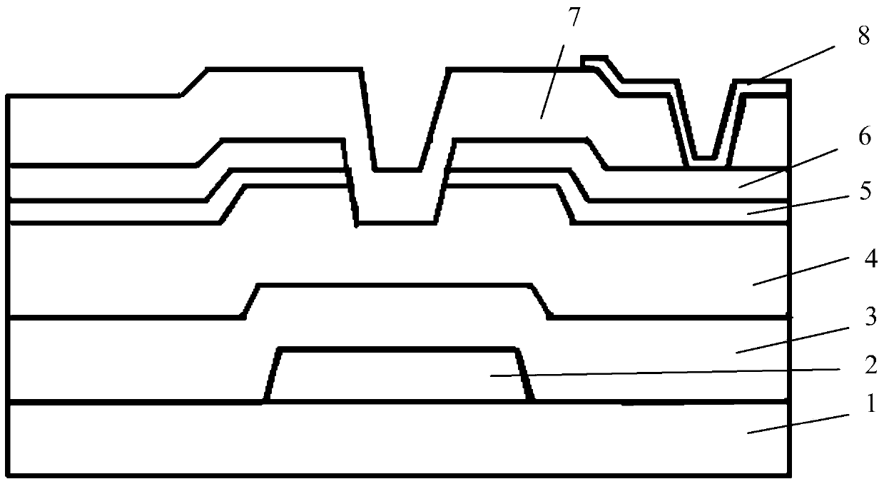
[0062]figure 1 A schematic diagram of the structure of a thin film transistor is provided, see figure 1 , the thin film transistor includes: a substrate 1 , a gate electrode 2 , a gate insulating layer 3 , and an active layer 4 , and the gate insulating layer 3 is interposed between the gate electrode 2 and the active layer 4 .

[0063] In this embodiment, the thin film transistor may further include: an ohmic contact layer 5 , a source-drain electrode 6 , a passivation layer 7 , and a pixel electrode 8 . These layers are only examples, and more layer structures or less layer structures may be included in actual implementation.

[0064] In this embodiment, the gate electrode 2 can be made of copper, aluminum and other materials by spu...


PUM


Abstract

The invention discloses a thin film transistor, a manufacturing method thereof, an array substrate and a display device, which belongs to the technical field of thin film transistors. The thin film transistor comprises a substrate, a gate electrode, a gate insulation layer and an active layer. The gate insulation layer comprises an inner defect prevention layer and an interface defect prevention layer, wherein the inner defect prevention layer is located between the interface defect prevention layer and the gate electrode; the inner defect prevention layer is used for reducing inner defects of the gate insulation layer; and the interface defect prevention layer is used for reducing defects of a contact interface between the gate insulation layer and the active layer. Through arranging the gate insulation layer in the above mode, the defect number of the inner part of the gate insulation layer and the defect number of the contact surface between the gate insulation layer and the active layer can be reduced, accumulation of carriers (positrons) inside the gate insulation layer and on the contact surface between the gate insulation layer and the active layer can thus be reduced, thin film transistor threshold voltage offset phenomena can be effectively reduced, and the defect rate of the thin film transistors is reduced.

Description

technical field [0001] The invention relates to the technical field of thin film transistors, in particular to a thin film transistor and a preparation method thereof, an array substrate, and a display device. Background technique [0002] A thin film transistor (Thin Film Transistor, referred to as "TFT") is a key device in a liquid crystal display device, and plays a very important role in the performance of the display device. [0003] Existing thin film transistors mainly include a gate electrode, a gate insulating layer, an active layer, an ohmic contact layer, a source-drain electrode, a passivation layer, and a pixel electrode that are sequentially stacked on a substrate. [0004] Under light conditions, the existing thin film transistors will generate photo-generated carriers, which will accumulate in the defect states in the gate insulating layer or in the defect states at the interface between the gate insulating layer and the active layer, thereby forming thin fil...

Claims


Application Information

Patent Timeline
Patent Type & Authority Patents(China)
IPC IPC(8): H01L29/786H01L29/423H01L21/336H01L21/28H01L27/12
CPCH01L27/1214H01L29/401H01L29/42384H01L29/66742H01L29/786
Inventor 李正亮周斌姚琪孙雪菲高锦成张伟张斌曹占锋
Owner BOE TECH GRP CO LTD
Why Eureka
Try Eureka