Virtual IO inter-chip connection circuit for FPGAs

An interconnection circuit and chip-to-chip technology, which is applied in the field of FPGA virtual IO chip interconnection circuits, can solve the problems of low IC design verification, high bit error rate transmission, and low bandwidth, so as to reduce the bit error rate, The effect of ensuring accurate transmission, increasing speed and bandwidth

Active Publication Date: 2015-10-21
无锡亚科鸿禹电子有限公司
View PDF4 Cites 12 Cited by
  • Summary
  • Abstract
  • Description
  • Claims
  • Application Information

AI Technical Summary

Problems solved by technology

However, the low bandwidth, low rate, and high bit error rate transmission caused by the low-frequency standard clock and fixed data bit width seriously limit the application environment of this technical solution, which is not very helpful for IC design verification.

Method used


Image

  • Virtual IO inter-chip connection circuit for FPGAs
  • Virtual IO inter-chip connection circuit for FPGAs
  • Virtual IO inter-chip connection circuit for FPGAs

Examples


Embodiment Construction

[0024] In order to make the above objects, features and advantages of the present invention more comprehensible, the present invention will be further described in detail below in conjunction with the accompanying drawings and specific embodiments.

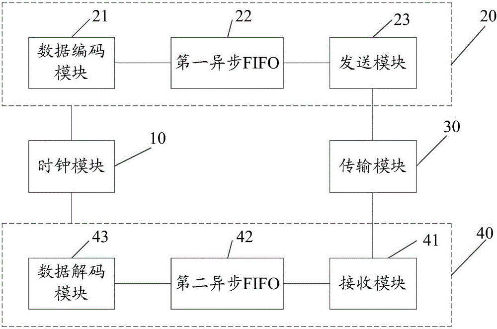
[0025] One of the core concepts of the embodiments of the present invention is to provide a cross-clock domain-oriented FPGA virtual IO inter-chip interconnection scheme, so that the transmission bandwidth and transmission rate can be arbitrarily increased in a large range, and the error rate can be greatly reduced. The code rate, thus bringing convenience to the operation of the FPGA interconnection interface.

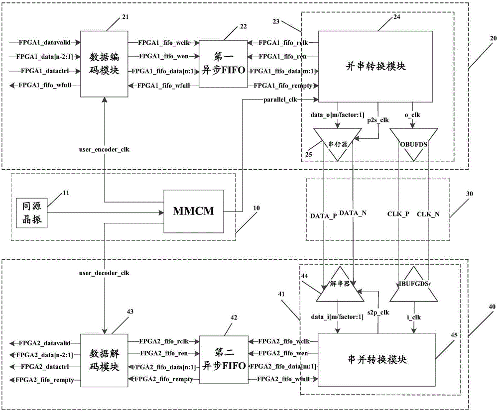
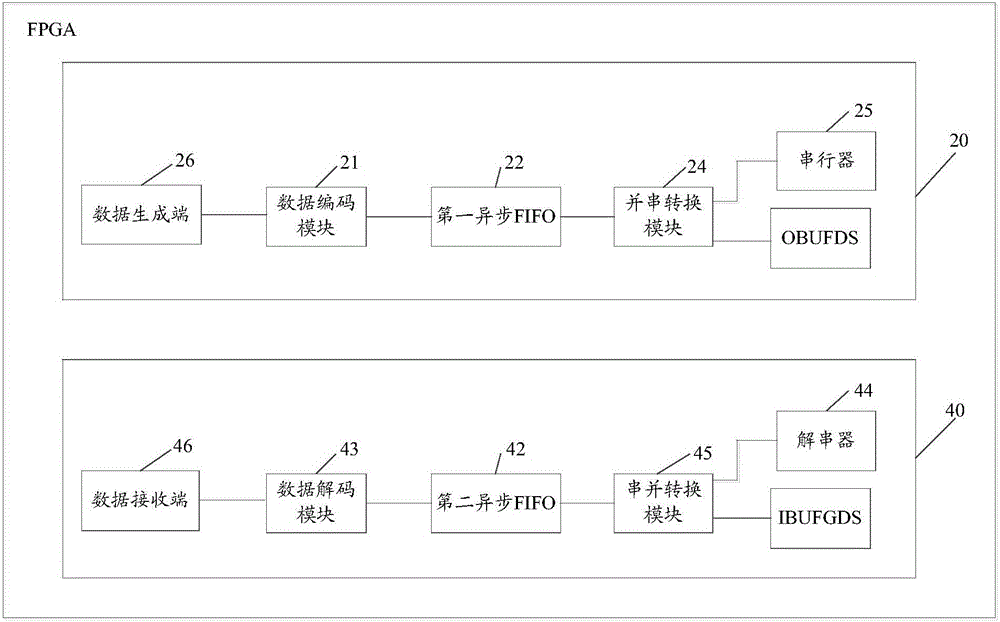
[0026] refer to figure 1 , shows a structural block diagram of a FPGA virtual IO chip interconnection circuit embodiment of the present invention, specifically may include the following modules: clock module 10, sending FPGA end circuit 20 such as FPGA, transmission module 30 and receiving FPGA end circuit 40 For example...


PUM


Abstract

The present invention provides a virtual IO inter-chip connection circuit for FPGAs. The circuit comprises a clock module, a sending FPGA end circuit, a transmission module and a receiving FPGA end circuit. The sending FPGA end circuit comprises a data coding module for generating coded data; a first asynchronous FIFO which caches coded data written by the data coding module according to a coding clock and an asynchronous FIFO write protocol; and a sending module which sends data of at least two bits and a differential serial clock read from the first asynchronous FIFO until all the coded data is sent. The receiving FPGA end circuit comprises a receiving module for receiving the data of at least two bits and the differential serial clock until all the coded data is received; a second asynchronous FIFO which caches the data of at least two bits written by the receiving module according to the asynchronous FIFO write protocol and the differential serial clock until all the coded data is written; and a data decoding module which decodes the coded data synchronously. According to the invention, the transmission bandwidth and the transmission rate can be increased arbitrarily within a considerable range while the bit error rate can be reduced greatly.

Description

technical field [0001] The invention relates to the field of communication technology, in particular to an FPGA virtual IO chip interconnection circuit. Background technique [0002] Since the launch of the world's first FPGA (Field-Programmable Gate Array, Field Programmable Gate Array) product in 1985, FPGA has begun to occupy the mainstream of IC (Integrated Circuit, integrated circuit) design verification, relying on its unique advantages to start Gradually replace individual custom chips. At the same time, with the rapid development of the microelectronics industry, the logic resources required for IC design verification are also increasing rapidly. The logic resources of a single FPGA often cannot meet the needs of IC design verification. At this time, it is necessary to interconnect two or more FPGAs to expand resources, but because the interconnection between FPGAs occupies too many interface IOs (Input / Output, input / output), it seriously limits the development of IC...

Claims


Application Information

Patent Timeline
Patent Type & Authority Applications(China)
IPC IPC(8): G06F13/40
CPCG06F13/4068
Inventor 吴沙杨滔
Owner 无锡亚科鸿禹电子有限公司
Why Eureka
Try Eureka