Pattern reconfigurable antenna based on frequency selective surface of graphene composite structure
A graphene composite and structural frequency technology, applied to antennas, electrical components, etc., can solve the problem of inability to flexibly change the antenna gain and beam width, and achieve the effect of changing the beam width and increasing the gain
- Summary
- Abstract
- Description
- Claims
- Application Information
AI Technical Summary
Problems solved by technology
Method used
Image
Examples
Embodiment 1
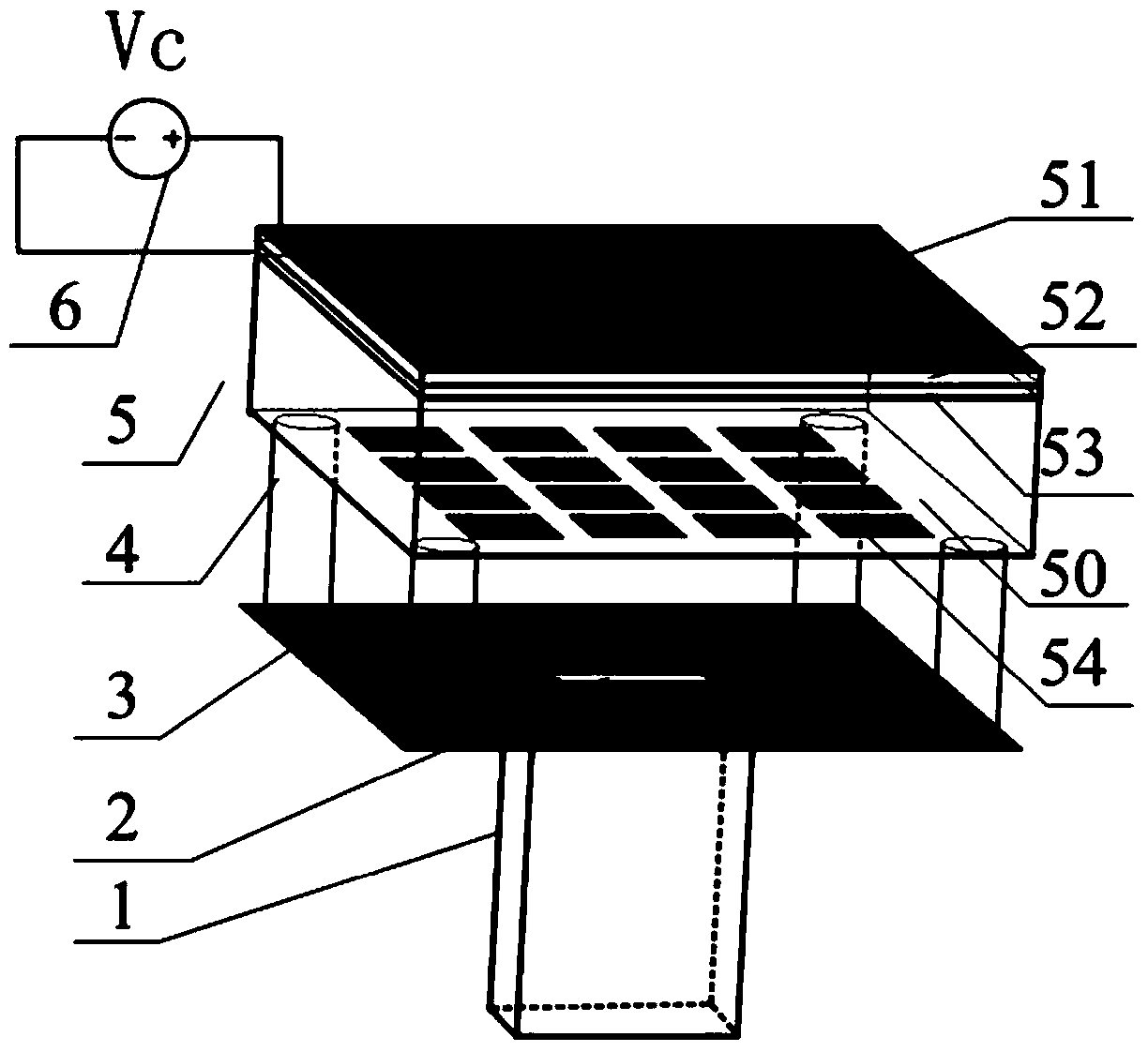
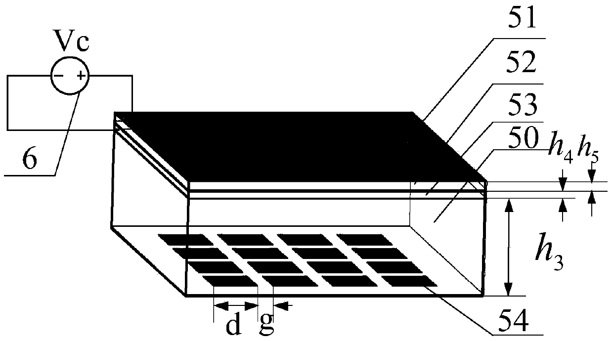
[0040] refer to figure 1 , the present invention includes a rectangular waveguide feeder 1, a rectangular radiation unit 2, a reflector 3, four support columns 4, a frequency selective surface 5 and a DC bias Vc6, wherein the frequency selective surface 5 includes a dielectric substrate 50, pasted on the upper surface of the dielectric substrate The graphene composite structure and the square patch array 54 printed on the lower surface of the dielectric substrate, the graphene composite structure is composed of a graphene layer 51, an aluminum oxide layer 52 and a polysilicon layer 53 stacked sequentially from top to bottom. Between the layer 51 and the polysilicon layer 53, a DC bias voltage Vc6 is added to regulate the surface conductivity of graphene; the aluminum oxide layer 52 in the graphene composite structure is used to isolate the polysilicon layer 53 and the graphene layer 51, forming a bias pressure; the frequency selective surface 5 is fixed on the top of the refle...
Embodiment 2
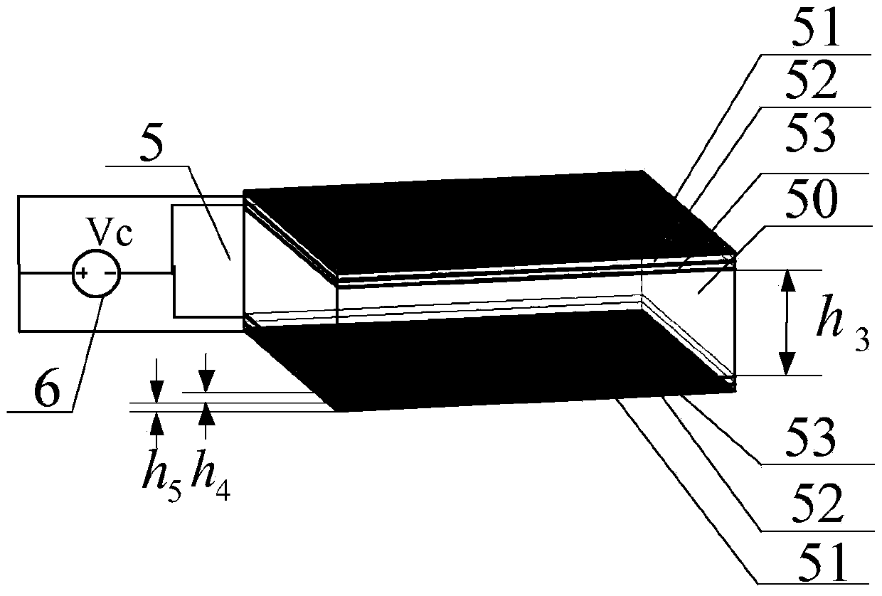
[0049] Embodiment 2 except the structure of the frequency selective surface, other structures are the same as embodiment 1, and the structural diagram of the frequency selective surface adopted in embodiment 2 is as follows image 3 as shown,
[0050] refer to image 3 , the frequency selective surface in this embodiment is only to replace the square patch array 54 originally printed on the lower surface of the dielectric substrate with a graphene composite structure, next to the dielectric substrate is a polysilicon layer 53, followed by an aluminum oxide layer 52 and graphene layer 51; the width of this composite structure is identical with reflective plate 3 widths, and the thickness of dielectric substrate is identical with embodiment 1 h 3 =4.5mm, the thickness is determined by the working wavelength λ in the medium g decision, the approximate formula is h 3 =λ g / 2; supporting column 4, reflector 3, rectangular radiation unit 2, and rectangular waveguide feeder 1 are...
PUM
 Abstract
Description
Claims
Application Information


