Substrates for power modules, substrates for power modules with built-in heat sinks, and power modules

A power module and heat sink technology, which is applied in the direction of electric solid state devices, circuit heating devices, semiconductor devices, etc., can solve the problems of inability to promote heat dissipation, inability to form cooling capacity, insufficient heat sink strength, etc., and achieve excellent power cycle characteristics, Effects of suppressing cracks and effectively dissipating heat

Active Publication Date: 2017-12-01
MITSUBISHI MATERIALS CORP
View PDF11 Cites 0 Cited by
  • Summary
  • Abstract
  • Description
  • Claims
  • Application Information

AI Technical Summary

Problems solved by technology

Therefore, the radiator itself is not strong enough and it is very difficult to handle
[0017] In addition, since the heat sink is formed by casting, the structure of the heat sink becomes relatively simple, and a heat sink with high cooling capacity cannot be formed, and there is a problem that heat dissipation cannot be promoted.

Method used


Image

  • Substrates for power modules, substrates for power modules with built-in heat sinks, and power modules
  • Substrates for power modules, substrates for power modules with built-in heat sinks, and power modules
  • Substrates for power modules, substrates for power modules with built-in heat sinks, and power modules

Examples


Embodiment 1

[0148] A comparative experiment performed to confirm the effectiveness of the present invention will be described.

[0149] As shown in Table 1, bond the insulating substrate, the aluminum plate serving as the first aluminum layer of the circuit layer, the copper plate serving as the first copper layer, the aluminum plate serving as the second aluminum layer of the metal layer, and the copper plate serving as the second copper layer. To produce substrates for power modules.

[0150] The size of the circuit layer is 37mm×37mm, the size of the insulating substrate is 40mm×40mm, and the size of the metal layer is 37mm×37mm.

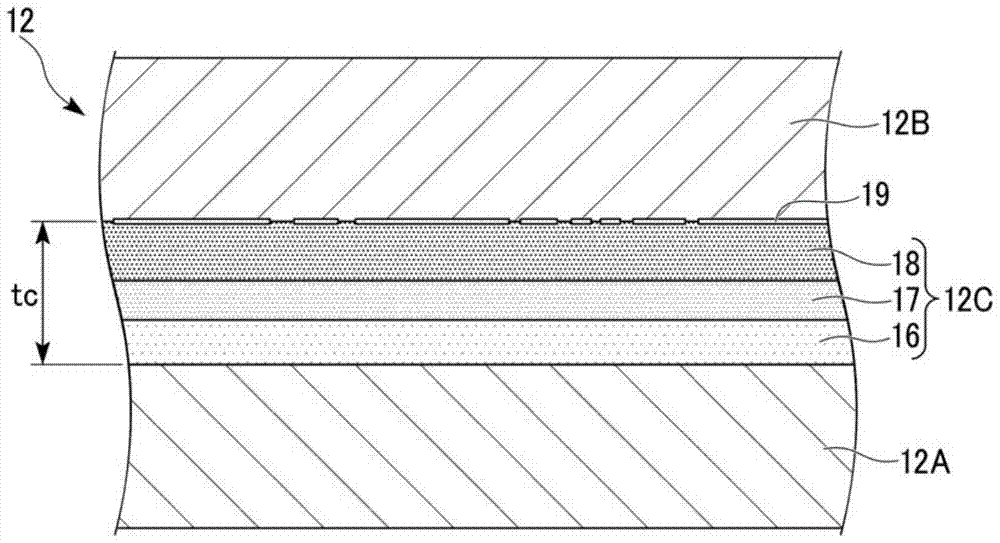
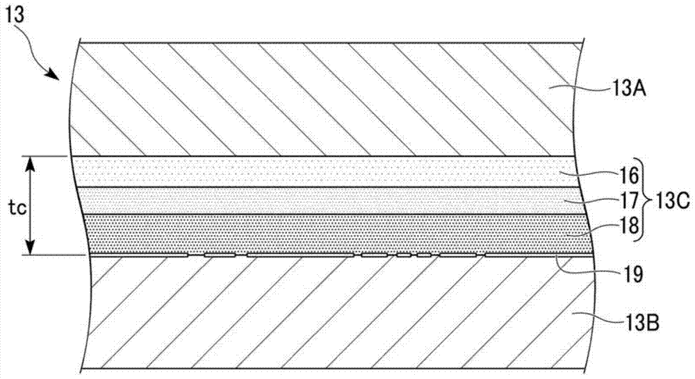
[0151] "TLP" shown in Table 2, by adding Cu to 1.0mg / cm 2 fixed on the surface of the insulating substrate, and on the stacking side with 5kgf / cm 2 In the pressurized state, at 10 -3 In a vacuum of Pa, the aluminum plate and the insulating substrate were bonded by heating at a temperature of 600° C. for 30 minutes.

[0152] "Al-Si brazing" shown in Table...

Embodiment 2

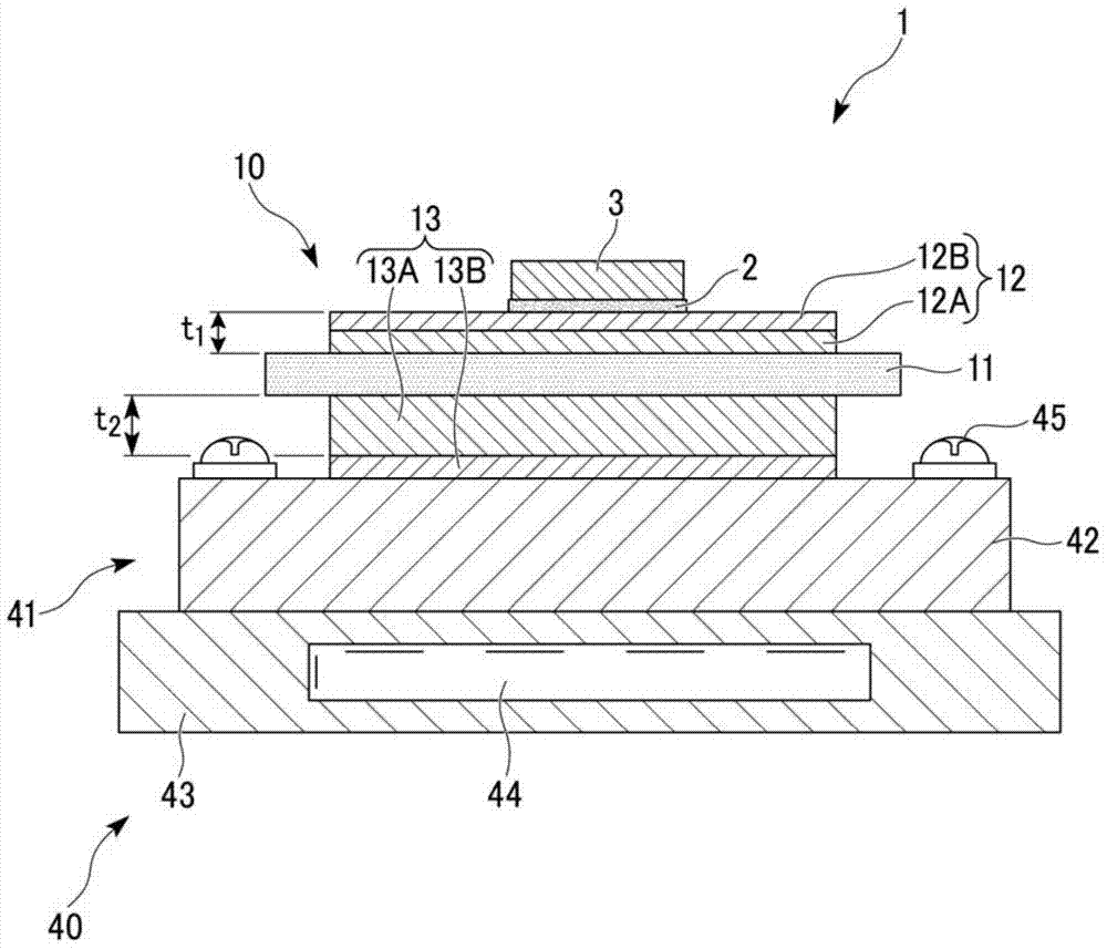
[0181] Next, as in the above-mentioned second embodiment and Figure 6 As shown in , the metal layer of the power module substrate and the heat sink were joined via the second solder layer, and the joining rate of the second solder layer was evaluated.

[0182] As shown in Table 3, an insulating substrate, an aluminum plate as the first aluminum layer of the circuit layer, a copper plate as the first copper layer, an aluminum plate as the second aluminum layer as the metal layer, and a copper plate as the second copper layer were fabricated to produce a power Module substrate.

[0183] The size of the circuit layer is 37mm×37mm, the size of the insulating substrate is 40mm×40mm, and the size of the metal layer is 37mm×37mm.

[0184] In addition, "TLP" and "Al-Si brazing" shown in Table 4 were made into the same joining method as Example 1 and Table 2 mentioned above.

[0185] In addition, a heat sink is bonded to the other side of the metal layer of the power module substrat...


PUM

PropertyMeasurementUnit
thicknessaaaaaaaaaa
thicknessaaaaaaaaaa

Abstract

The present invention provides a power module comprising an insulating substrate (11), a circuit layer (12) formed on one side of the insulating substrate (11), and a metal layer (13) formed on the other side of the insulating substrate (11) A substrate (10), wherein the circuit layer (12) has a first aluminum layer (12A) made of aluminum or an aluminum alloy bonded to the insulating substrate (11), and a solid phase diffusion bonded to the first aluminum layer (12A). The aluminum layer (12A) has a first copper layer (12B) made of copper or a copper alloy, the metal layer (13) has a second aluminum layer (13A) made of aluminum or an aluminum alloy, and the circuit layer (12 ) The relationship between the thickness t1 of the metal layer (13) and the thickness t2 of the second aluminum layer (13A) is t1<t2.

Description

technical field [0001] The present invention relates to a substrate for a power module used in a semiconductor device for controlling large current and high voltage, a substrate for a power module with a heat sink, and a power module. [0002] This application claims priority based on Patent Application No. 2013-072677 filed in Japan on March 29, 2013 and Patent Application No. 2013-216802 filed in Japan on October 17, 2013, and uses the contents thereof here. Background technique [0003] Among semiconductor elements, since power semiconductor elements for supplying electric power generate relatively high heat, as a substrate on which the power semiconductor elements are mounted, for example, a power module substrate including a circuit layer and a metal layer is used. Made of AlN (aluminum nitride), Al 2 o 3 (alumina), Si 3 N 4 An insulating substrate made of (silicon nitride) or the like is formed by bonding a first metal plate to one side, and the metal layer is form...

Claims


Application Information

Patent Timeline
Patent Type & Authority Patents(China)
IPC IPC(8): H01L23/373H01L25/07H01L25/18
CPCH01L23/36H01L23/3735H01L23/4006H01L23/473H01L2224/32225H01L2924/13055B23K1/0016B23K1/19B23K20/023C04B35/645C04B37/021C04B37/026C04B2235/6562C04B2235/6581C04B2237/121C04B2237/124C04B2237/125C04B2237/127C04B2237/128C04B2237/343C04B2237/366C04B2237/368C04B2237/402C04B2237/407C04B2237/704C04B2237/706C04B2237/708C04B2237/86B23K2101/40B23K2103/10B23K2103/12B23K2103/18H05K1/0203H05K1/09H05K1/181H05K2201/066
Inventor 长友义幸寺崎伸幸黑光祥郎
Owner MITSUBISHI MATERIALS CORP
Why Eureka
Try Eureka