Vertically stacked image sensor

An image sensor, vertical stacking technology, applied in the field of image sensors, can solve the problem of image sensors with reduced resolution

Active Publication Date: 2015-10-28
APPLE INC
View PDF6 Cites 37 Cited by
  • Summary
  • Abstract
  • Description
  • Claims
  • Application Information

AI Technical Summary

Problems solved by technology

Therefore, many cameras of portable devices may have image sensors with reduced resolution so that they can be as small as possible

Method used


Image

  • Vertically stacked image sensor
  • Vertically stacked image sensor
  • Vertically stacked image sensor

Examples


Embodiment Construction

[0064] overview

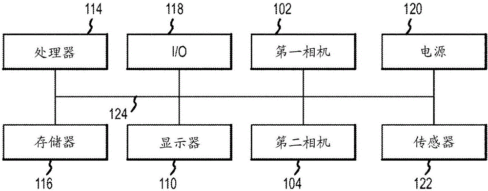
[0065] The disclosure may take the form of image sensors for cameras and other electronic devices. Many embodiments of the present disclosure include an image sensor with transmission gates to communicate between photodiodes in the image sensor and readout circuitry for those photodiodes. In some embodiments, transmission gates may be vertically oriented (as described in more detail below), and in other embodiments, transmission gates may be horizontally oriented. The orientation of the transfer gate can be selected based on the desired embodiment to implement and the desired size, shape and functionality of the image sensor.

[0066] In some embodiments, an image sensor may include a pixel array having two or more chips stacked together and interconnected using vertical gate structures. In other words, the pixel array can be split into two chips, for example, one chip has photodiodes and the other chip has readout circuitry and transistor arrays. For ex...


PUM

PropertyMeasurementUnit
thicknessaaaaaaaaaa
thicknessaaaaaaaaaa

Abstract

A vertically stacked image sensor having a photodiode chip and a transistor array chip. The photodiode chip includes at least one photodiode and a transfer gate extends vertically from a top surface of the photodiode chip. The image sensor further includes a transistor array chip stacked on top of the photodiode chip. The transistor array chip includes the control circuitry and storage nodes. The image sensor further includes a logic chip vertically stacked on the transistor array chip. The transfer gate communicates data from the at least one photodiode to the transistor array chip and the logic chip selectively activates the vertical transfer gate, the reset gate, the source follower gate, and the row select gate.

Description

[0001] Cross References to Related Applications [0002] This Patent Cooperation Treaty patent application claims priority to U.S. nonprovisional patent application 13 / 756,459, filed January 31, 2013, and entitled "Vertically Stacked Image Sensor," the contents of which are incorporated herein by reference in their entirety . technical field [0003] The present invention relates generally to electronic devices, and more particularly to image sensors for electronic devices. Background technique [0004] Cameras and other image recording devices typically use one or more image sensors, such as Charge Coupled Device (CCD) sensors or Complementary Metal-Oxide-Semiconductor (CMOS) image sensors. A typical CMOS image sensor may include a two-dimensional array of pixels, where each pixel may include a light detector, such as a photodiode, and one or more transistors that activate each pixel. The image sensor can be implemented in a rolling shutter configuration or a global shutt...

Claims


Application Information

Patent Timeline
Patent Type & Authority Applications(China)
IPC IPC(8): H01L27/146H01L29/78H01L29/786
CPCH01L27/14643H01L27/14634H01L27/1464H01L27/14641H01L29/7827H04N9/045H01L27/14614H01L27/14616H01L27/14638H01L27/14654H01L27/14843H04N25/70H04N25/79H04N25/134H01L27/146H04N25/00
Inventor 范晓峰
Owner APPLE INC
Why Eureka
Try Eureka