Display panel and repairing method thereof

A display panel and substrate technology, applied to static indicators, organic semiconductor devices, instruments, etc., can solve problems such as dark spots, pixel units that cannot emit light, and cumbersome processes

Inactive Publication Date: 2015-11-04
AU OPTRONICS CORP
View PDF6 Cites 59 Cited by
  • Summary
  • Abstract
  • Description
  • Claims
  • Application Information

AI Technical Summary

Problems solved by technology

At present, the light-emitting diodes used in the light-emitting diode display panel are embedded in each pixel unit on the substrate by pick and place after the respective fabrication is completed, and when any one of the light-emitting diodes is damaged or falls off during the process, Then this pixel unit will not be able to emit light and cause dark spots
However, the repetitive work of display panels is not easy and the process is cumbersome, so establishing a simple and fast repair method for LED display panels is the current direction of industry efforts

Method used


Image

  • Display panel and repairing method thereof
  • Display panel and repairing method thereof
  • Display panel and repairing method thereof

Examples


Embodiment Construction

[0070] In order for those skilled in the art to have a better understanding of the present invention, the preferred embodiments of the present invention are listed below, together with the attached drawings and descriptions, the composition of the present invention and the intended effects are described in detail.

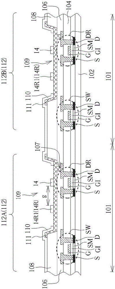
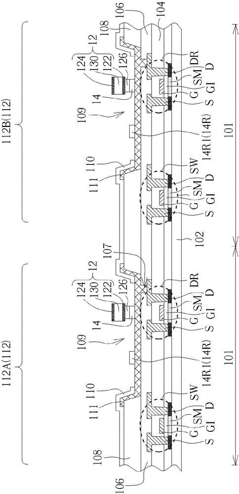
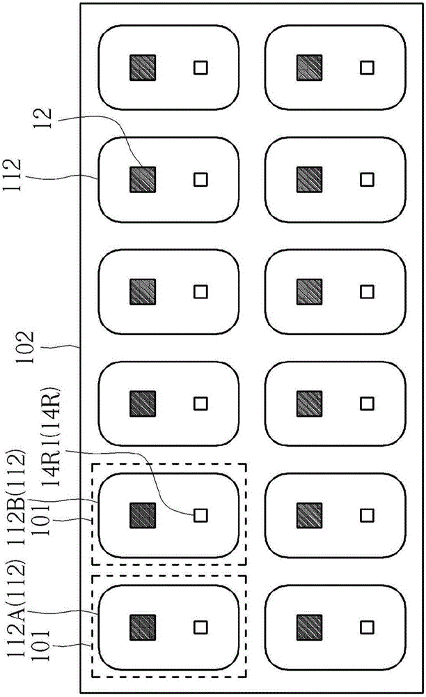
[0071] Please refer to Figure 1 to Figure 4 . figure 1 and figure 2 A schematic diagram illustrating a manufacturing method of a display panel according to a first embodiment of the present invention, image 3 depicts a top view of the display panel of the first embodiment of the present invention, Figure 4 An equivalent circuit diagram of the display panel of the present invention is shown. Such as figure 1 As shown, firstly, a substrate 102 is provided, and the substrate 102 includes a plurality of pixel regions 101 . The substrate 102 of this embodiment may include a rigid substrate or a flexible substrate, such as a glass substrate or a plastic substrat...


PUM


Abstract

The invention provides a display panel and a repairing method thereof. The repairing method comprising the steps of: a) providing a display panel, which comprises a substrate and a plurality of pixel units. The plurality of pixel units are disposed on the substrate, wherein each pixel unit comprises at least one connection pad, the at least one light-emitting element and at least a first alternate connection pad, the connection pad is provided on the substrate, the light emitting element is disposed on the connection pad and pad electrically connected with the connection, and the first backup connection pad is provided on the substrate and the connection pads electrically connected; 2) a testing process to determine whether the light emitting element is in an abnormal state function; and 3) a repair process, when detecting that the light emitting element of a pixel unit functional abnormality, there is provided a first light emitting element so as to form a first alternate alternate abnormality in the light emitting element having a function of pixel cells connected to the pad. Through the repair method, each pixel unit Jieneng normal operation and emits preset light color.

Description

technical field [0001] The invention relates to a display panel and a repair method thereof, in particular to a display panel with spare connection pads reserved and a repair method thereof. Background technique [0002] In recent years, with the advancement of technology and the development of the optoelectronic industry, electronic products such as PDA (personal digital assistant, PDA), mobile phone (mobile phone), smart phone (smart phone) and notebook computer (notebook, NB), etc. The use of products is becoming more and more common. As users' demand for electronic products increases day by day, display panels, which play an important role in electronic products, have also become the focus of designers. [0003] Light emitting diodes (light emitting diodes, LEDs) have been widely used in display panels due to their advantages of environmental protection, high photoelectric conversion efficiency, small size, long life, fixed wavelength and low heat generation. For examp...

Claims


Application Information

Patent Timeline
Patent Type & Authority Applications(China)
IPC IPC(8): G09F9/33
CPCG09G3/3233G09G2330/10H01L25/0753H10K59/12H10K71/861
Inventor 陈振彰徐文斌刘品妙
Owner AU OPTRONICS CORP
Why Eureka
Try Eureka