Fine pitch copper cylinder dimpling point preparation technology

A preparation process and micro-bump technology, which is used in semiconductor/solid-state device manufacturing, electrical components, electrical solid-state devices, etc., can solve problems such as low efficiency and achieve the effect of improving production efficiency

Inactive Publication Date: 2015-11-04
NAT CENT FOR ADVANCED PACKAGING
View PDF2 Cites 3 Cited by
  • Summary
  • Abstract
  • Description
  • Claims
  • Application Information

AI Technical Summary

Problems solved by technology

The biggest advantage of this process is that the cost is very low. However, the process is not yet mature, and it is also performed on a single chip, so the efficiency is low.

Method used


Image

  • Fine pitch copper cylinder dimpling point preparation technology
  • Fine pitch copper cylinder dimpling point preparation technology
  • Fine pitch copper cylinder dimpling point preparation technology

Examples


Embodiment Construction

[0030] The present invention will be further described below in conjunction with specific drawings.

[0031] The fine-pitch copper pillar micro-bump preparation process comprises the following steps:

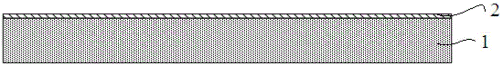
[0032] (1) if figure 1 As shown, a Ti / Cu seed layer 2 is electroplated on the surface of the wafer 1, and the thickness of the Ti / Cu seed layer 2 is 100-300 nm;

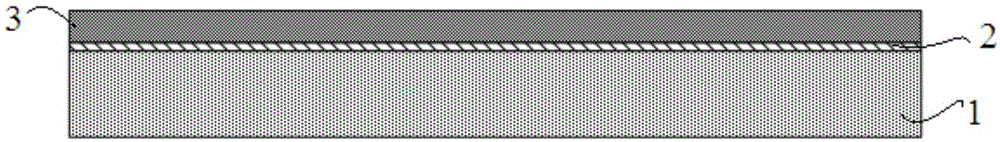
[0033] (2) if figure 2 As shown, the copper layer 3 is deposited on the surface of the Ti / Cu seed layer 2 by means of electroless plating or electroplating, and the thickness of the copper layer 3 is set according to needs, generally 10-100 μm;

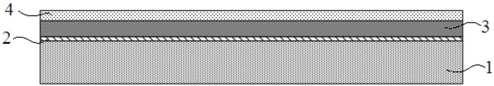
[0034] (3) if image 3 As shown, a solder layer 4 is prepared on the surface of the copper layer 3, the thickness of the solder layer 4 is 10-100 μm, and the material of the solder layer 4 is SnPb, SnAg, SnAgCu, SnBi or ternary or multi-component solder with alloy elements added ;

[0035] (4) if Figure 4 As shown, a photoresist layer 5 is coated on the surface of the ...


PUM

PropertyMeasurementUnit
thicknessaaaaaaaaaa
thicknessaaaaaaaaaa
distanceaaaaaaaaaa

Abstract

The invention relates to one kind of fine pitch copper cylinder dimpling point preparation technology characterized in that the following steps are comprised: (1), a Ti/Cu seed layer is electroplated on the surface of a wafer; (2) a copper layer is deposited on the surface of the Ti/Cu seed layer; (3), a brazing filler metal layer is prepared on the surface of the copper layer; (4), a photoresist layer is coated on the surface of the brazing filler metal layer; (5), opening technology is applied on the photoresist layer to form openings which extend from the upper surface of the photoresist layer to the lower surface of the photoresist layer; the size, the quantity and the distribution of the photoresist layer saved after opening making are consistent with the size, the quantity and the distribution of copper columns which need to be made; (6), etching is carried out on the opening portions, and the brazing filler metal layer, the copper layer and the Ti/Cu seed layer below the opening is etched to expose the upper surface of the wafer; (7), the residual photoresist layer is peeled off; and (8) backflows enable copper column dimpling points to form. According to the invention, preparation of the copper column dimpling points can be completed in batch; the production efficiency is raised; dimpling point manufacturing of ternary or multicomponent alloy materials so as to satisfy application of different products.

Description

technical field [0001] The invention relates to a fine-pitch copper pillar micro-bump preparation process, which belongs to the technical field of high-density electronic packaging. Background technique [0002] With the continuous increase of IC chip bandwidth, more and more I / O ports need to be drawn out. Traditional micro-bump technology and wire bonding technology have been difficult to meet the needs of high-bandwidth IC chips. Therefore, fine-pitch, high-density micro-bump technology has begun to be widely used. In the micro-bump structure, copper pillar bump technology is the most widely used. Since Intel first used it in processors in 2006, copper pillar bumps have gradually been widely used in wafer-level bump manufacturing and micro-assembly processes of Flip-chip (flip-chip) technology. Copper pillar bump is composed of copper pillar and top solder cap, which has a height-to-diameter ratio greater than 1:1, while the proportion of solder cap is small, and the c...

Claims


Application Information

Patent Timeline
Patent Type & Authority Applications(China)
IPC IPC(8): H01L21/60
CPCH01L24/11H01L2224/11462H01L2224/11622
Inventor 何洪文于大全孙鹏曹立强
Owner NAT CENT FOR ADVANCED PACKAGING
Why Eureka
Try Eureka