Supercharge Your Innovation With Domain-Expert AI Agents!

Method of forming memory element

A technology of memory components and resistance conversion layers, which is applied in the direction of electrical components, can solve the problems of low pass rate and efficiency of resistive non-volatile memory, and achieve the goal of setting current stability, improving efficiency, and improving pass rate and efficiency Effect

Active Publication Date: 2017-10-13
WINBOND ELECTRONICS CORP
View PDF3 Cites 0 Cited by
  • Summary
  • Abstract
  • Description
  • Claims
  • Application Information

AI Technical Summary

Problems solved by technology

[0005] The technical problem solved by the present invention is to provide a method for forming a memory element to solve the problem of low pass rate and low efficiency of resistive non-volatile memory in the prior art

Method used


Image

  • Method of forming memory element
  • Method of forming memory element
  • Method of forming memory element

Examples


Embodiment Construction

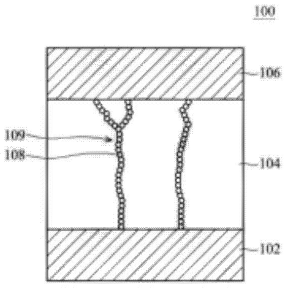
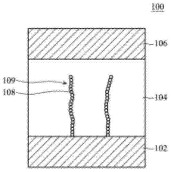
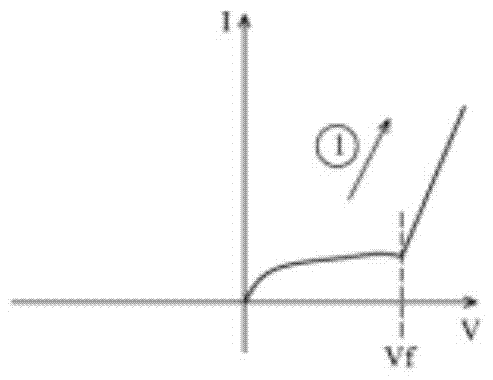
[0025] The fabrication and use of the embodiments of the present invention will be described in detail below. It should be noted, however, that this application presents many applicable inventive concepts, which can be embodied in a wide variety of specific forms. The specific embodiments listed herein are only the specific ways of making and using the present invention, and are not intended to limit the protection scope of the present invention. In addition, in practical applications, the execution of the first manufacturing process and the second manufacturing process may include the situation where the second manufacturing process is performed immediately after the first manufacturing process, or may include In the case of additional manufacturing processes. Elements may be arbitrarily drawn in different scales. This is done merely for simplicity and clarity of drawing the various elements. In addition, when a first material layer is located on a second material layer, i...


PUM


Abstract

The invention provides a formation method of a memory component. The method comprises the following steps that a resistance transformation layer is formed on a first electrode; a second electrode is formed on the resistance transformation layer; a formation voltage is provided for the resistance transformation layer so that a resistance of the resistance transformation layer is decreased; after the formation voltage is provided, an initial reset voltage is provided for the resistance transformation layer so that the resistance of the resistance transformation layer is increased; after the initial reset voltage is provided, a first setting voltage is provided for the resistance transformation layer so that the resistance of the resistance transformation layer is decreased; after the first setting voltage is provided, a second reset voltage is provided for the resistance transformation layer so that the resistance of the resistance transformation layer is increased; and after the second reset voltage is provided, a second setting voltage is provided for the resistance transformation layer so that the resistance of the resistance transformation layer is decreased, wherein the second setting voltage is less than the first setting voltage. By using the method of the invention, a qualified rate and efficiency of a resistance-type nonvolatile memory are increased.

Description

technical field [0001] The present invention relates to a method for forming a memory element, in particular to a method for forming a resistive memory element. Background technique [0002] In recent years, various consumer electronic products have become popular, which has greatly increased the demand for non-volatile memory. Flash memory (Flash Memory) is the mainstream of non-volatile memory. However, as the size of components continues to shrink, flash memory has encountered disadvantages such as high operating voltage, slow operation speed, and poor data retention, which limit the future development of flash memory. [0003] Accordingly, many new non-volatile memory materials and devices are currently being actively developed. Modern non-volatile memory devices include Magnetic Random Access Memory (MRAM), Phase Change Memory (PCM), and Resistive Random Access Memory (RRAM). Among them, resistive non-volatile memory has the advantages of low power consumption, low o...

Claims


Application Information

Patent Timeline
Patent Type & Authority Patents(China)
IPC IPC(8): H01L45/00
Inventor 林孟弘吴伯伦
Owner WINBOND ELECTRONICS CORP
Features
  • R&D
  • Intellectual Property
  • Life Sciences
  • Materials
  • Tech Scout
  • Unparalleled Data Quality
  • Higher Quality Content
  • 60% Fewer Hallucinations
Learn More