Locating System-on-Chip Sequential Logic Errors, Error Rate Calculation and Application Method

A sequential logic and system-on-chip technology, applied in the direction of measuring devices, instruments, measuring electronics, etc., can solve the problem of adding logic, etc., and achieve the effect of saving cost, increasing chip area and cost

Active Publication Date: 2018-08-28
SHANGHAI XINCHU INTEGRATED CIRCUIT
View PDF4 Cites 0 Cited by
  • Summary
  • Abstract
  • Description
  • Claims
  • Application Information

AI Technical Summary

Problems solved by technology

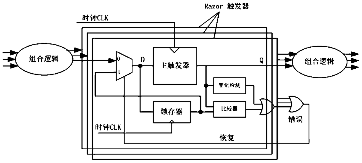
It can be seen from the above that the scan chain technology is a technology adopted to simplify chip testing, and has no effect on the function of the chip, but it will inevitably increase logic and have some impact on the chip

Method used


Image

  • Locating System-on-Chip Sequential Logic Errors, Error Rate Calculation and Application Method
  • Locating System-on-Chip Sequential Logic Errors, Error Rate Calculation and Application Method
  • Locating System-on-Chip Sequential Logic Errors, Error Rate Calculation and Application Method

Examples


Embodiment 1

[0044] DVFS technology is a method to optimize processor energy consumption, but changes in voltage and frequency will inevitably cause internal timing logic errors. User acceptable error rate means that under a specific condition (voltage V, frequency F, temperature T, etc.), the processor can avoid erroneous instructions and / or data when running the specific application program of the specific user; or It is said that under a specific condition (voltage V, frequency F, temperature T, etc.), the probability that some instructions and / or data will be wrong during all tests is not 100%. Once these instructions and / or data are wrong, the chip will The system where it resides can resume normal work under a specific recovery mechanism, and the recovery process caused by erroneous instructions and / or data does not affect the user's experience.

[0045] For example, a recovery mechanism using a watchdog circuit is as follows: enable and disable the watchdog before and after the prog...

Embodiment 2

[0061] According to the method for locating the sequential logic error of the system on chip proposed in the first embodiment, the present invention proposes a method for reducing the error rate of the sequential logic of the system on chip.

[0062] Instructions and / or data that have errors can be divided into two situations: one is 100% error occurrence rate, that is, all test results of the instruction and / or data under a certain test condition show that logic or timing has occurred Error; one is a non-100% error rate, that is, the instruction and / or data under a certain test condition, some test results show that no error occurs, and some do not occur error. Through the above grouping, users can choose those grouping chip products that are suitable for the working conditions of the customer's application environment and the appropriate power consumption budget. If user A wants the chip to meet the power consumption budget PBx (1≤x≤N), then it can work under the condition o...

Embodiment 3

[0067] According to the method for locating the SOC sequential logic error and the method for reducing the SOC sequential logic error rate proposed in the above embodiments, this embodiment further describes the specific application of the method for locating the SOC sequential logic error.

[0068] Assuming that the system chip on a chip is under the test conditions V1, T1, and F1, after adopting the test method of the multiplexed scan chain technology of the present invention, all instructions and / or data pass without error, as shown in the attached Figure 7 As shown, its power budget is PB1. Then the chip can be provided to some customer applications whose power consumption budget is above PB1. If the system-on-chip is under test conditions V2, T1, and F1 (V2


PUM


Abstract

The invention provides a method and an application for positioning system-on-chip temporal logic errors, and an error rate calculation method. When positioning a system-on-chip temporal logic error, a same test instruction and / or data are / is input into a P-level scan chain, an N-level pipeline and a Q-level scan chain through PAD ports under the same test condition, and test on the test instruction and / or data is achieved through controlling a scan chain enable signal. During the error rate calculation, an error rate of the test instruction and / or data in the environment is obtained according to all processing results. During the reduction of the error rate, a first test instruction and / or data replaces a second test instruction and / or data and achieves the function the same as that of the test instruction and / or data when a processor executes the second test instruction and / or data in the application. The user selects a chip within an error occurrence rate range acceptable by the user according to his application requirement, thereby saving cost and satisfying requirements of the user.

Description

technical field [0001] The invention relates to the technical field of locating system-on-chip timing logic errors, in particular to a method for locating system-on-chip timing logic errors, error rate calculation and application thereof. Background technique [0002] Dynamic voltage frequency scaling (Dynamic Voltage Frequency Scale, DVFS) technology is a method that can optimize processor energy consumption, which allows the processor to dynamically change its clock frequency and supply voltage during operation. This technique can be implemented at the software level as well as at the hardware level. At the hardware level, the direct consequence of voltage and frequency reduction is that sequential logic errors may occur, which will affect the normal operation of the processor. A traditional approach is to use a delay chain or a look-up table to determine the minimum voltage for error-free operation at a particular frequency. Another method is to add a delay error detect...

Claims


Application Information

Patent Timeline
Patent Type & Authority Patents(China)
IPC IPC(8): G01R31/3185
Inventor 景蔚亮陈邦明
Owner SHANGHAI XINCHU INTEGRATED CIRCUIT
Why Eureka
Try Eureka