Array substrate, display panel, display device and manufacturing method of array substrate

A technology of array substrate and substrate substrate, applied in semiconductor/solid-state device manufacturing, instruments, semiconductor devices, etc., can solve problems such as product yield decline

Inactive Publication Date: 2015-11-18
BOE TECH GRP CO LTD +1
View PDF5 Cites 21 Cited by
  • Summary
  • Abstract
  • Description
  • Claims
  • Application Information

AI Technical Summary

Problems solved by technology

Especially when the distance between the first data line 61' and the second data line 62' is

Method used


Image

  • Array substrate, display panel, display device and manufacturing method of array substrate
  • Array substrate, display panel, display device and manufacturing method of array substrate
  • Array substrate, display panel, display device and manufacturing method of array substrate

Examples


no. 1 example

[0105] combined below figure 2 , Figure 3a and Figure 3b The array substrate 1 according to the first embodiment of the present disclosure is described. figure 2 is a schematic top view of the array substrate 1 according to the first embodiment, Figure 3a is the edge of the array substrate 1 figure 2 A schematic cross-sectional view of the A-B line, and Figure 3b is the edge of the array substrate 1 figure 2 Schematic cross-sectional view of line C-D.

[0106] The array substrate 1 of the display panel includes gate lines 20 and data lines which are insulated from each other on the base substrate 10 and intersect to define a plurality of sub-pixel units 30 . A thin film transistor 40 and a pixel electrode 50 are formed in each sub-pixel unit 30 . The thin film transistor 40 includes a gate electrode 40a, a source electrode 40b, and a drain electrode 40c. The data lines include a first data line 61 and a second data line 62 arranged side by side between every tw...

no. 2 example

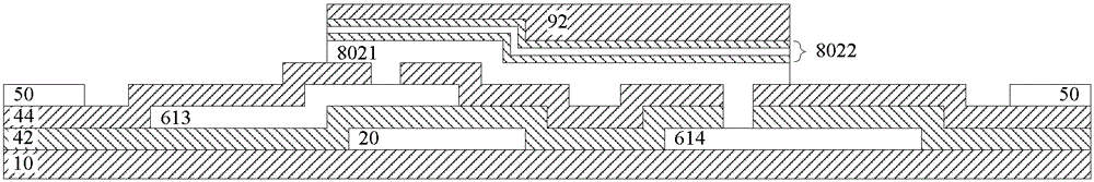
[0114] combined below Figure 4 , Figure 5a and Figure 5b An array substrate 2 according to a second embodiment of the present disclosure is described. Figure 4 is a schematic top view of the array substrate 2 according to the second embodiment, Figure 5a is the edge of the array substrate 2 Figure 4 A schematic cross-sectional view of the A-B line, and Figure 5b is the edge of the array substrate 2 Figure 4 Schematic cross-sectional view of line C-D.

[0115] The difference between the second embodiment and the first embodiment is that the first segment of the first data line is set on the same layer as the source / drain electrode of the thin film transistor, instead of being on the same layer as the gate electrode of the thin film transistor as in the first embodiment. layer settings.

[0116] Such as Figure 4 As shown, the first data line 61 includes a plurality of first segments 613 and second segments 614 arranged alternately. The first segment 613 is resp...

no. 3 example

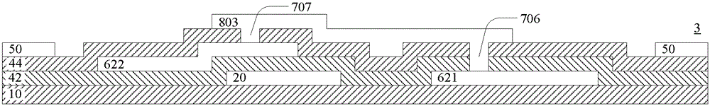
[0122] combined below Figure 6 , Figure 7a , Figure 7b , Figure 7c and Figure 7d An array substrate 3 according to a third embodiment of the present disclosure is described. Figure 6 is a schematic top view of the array substrate 3 according to the third embodiment, Figure 7a is the edge of the array substrate 3 Figure 6 A schematic cross-sectional view of the A-B line, Figure 7b is the edge of the array substrate 3 Figure 6 A schematic cross-sectional view of the G-H line, Figure 7c is the edge of the array substrate 3 Figure 6 A schematic cross-sectional view of line C-D, and Figure 7d is the edge of the array substrate 3 Figure 6 Schematic cross-sectional view of line E-F.

[0123] The difference between the third embodiment and the second embodiment is that the second data line includes segments arranged in a staggered manner, and each segment is arranged in a staggered layer with a corresponding segment of the first data line.

[0124] Such as ...


PUM


Abstract

The invention relates to the technical field of display and provides an array substrate, a display panel, a display device and a manufacturing method of the array substrate. The array substrate comprises grid lines and data lines insulated from one another on a lining substrate intersecting with each other to limit a plurality of sub pixel units. A thin film transistor and a pixel electrode are formed in each sub pixel unit. Each data line comprises a first data line body and a second data line body arranged between two columns of the corresponding adjacent sub pixel units side by side. In every two columns of the adjacent sub pixel units, the sub pixel units on the odd number line are connected with the corresponding first data line bodies, the sub pixel units on the even number line are connected with the corresponding second data line bodies, and at least part of first data line bodies and the adjacent second data line bodies are arranged on different layers between every two adjacent sub pixel units. According to the array substrate, the display panel, the display device and the manufacturing method of the array substrate, at least part of the first data lines and the adjacent corresponding second data lines are arranged on the different layers, and the short circuit between double data lines is solved.

Description

technical field [0001] The present disclosure relates to the field of display technology, and in particular to an array substrate, a display panel, a display device, and a method for manufacturing the array substrate. Background technique [0002] Currently, in various thin film transistor-liquid crystal display (TFT-LCD) products, the data lines need to be designed with double data lines to increase the signal output frequency. Such as figure 1 As shown, the display panel of the liquid crystal display device includes an array substrate 1'. The array substrate 1' includes gate lines 20' and data lines intersecting each other on a base substrate (not shown) and defining a plurality of sub-pixel units 30'. A thin film transistor 40' and a pixel electrode 50' are formed in each sub-pixel unit 30'. The thin film transistor 40' includes a gate electrode 40a', a source electrode 40b' and a drain electrode 40c'. The data lines include a first data line 61' and a second data lin...

Claims


Application Information

Patent Timeline
IPC IPC(8): G02F1/1362G02F1/1368H01L27/12H01L21/77
CPCG02F1/136227G02F1/136286G02F1/1368H01L27/124H01L27/1259G02F1/13629G02F1/134345G02F1/136295G02F1/134309G02F2201/123H01L27/127
Inventor 王守坤郭会斌冯玉春李梁梁郭总杰
Owner BOE TECH GRP CO LTD
Why Eureka
Try Eureka