Fabrication and package methods of high-efficiency heat-conduction semiconductor chip

A packaging method and semiconductor technology, applied in semiconductor/solid-state device manufacturing, semiconductor devices, semiconductor/solid-state device components, etc., can solve the problems of semiconductor chip heating and plug-in form affecting performance, reliability, stability, etc., to achieve Re-protection effect, practical convenience, effect of reducing the possibility of fire or explosion

Active Publication Date: 2015-11-18
BESTBRIGHT ELECTRONICS
View PDF5 Cites 3 Cited by
  • Summary
  • Abstract
  • Description
  • Claims
  • Application Information

AI Technical Summary

Problems solved by technology

[0004] The present invention solves the problems of heat generation of semiconductor chips and plug-in forms that affect performance, reliability, and stability, thereby providing a high-efficiency heat conduction method for manufacturing and packaging semiconductor chips with high efficiency heat conduction.

Method used


Image

  • Fabrication and package methods of high-efficiency heat-conduction semiconductor chip
  • Fabrication and package methods of high-efficiency heat-conduction semiconductor chip
  • Fabrication and package methods of high-efficiency heat-conduction semiconductor chip

Examples


Embodiment Construction

[0055] In order to make the technical problems, technical solutions and beneficial effects solved by the present invention clearer, the present invention will be further described in detail below in conjunction with the accompanying drawings and embodiments. It should be understood that the specific embodiments described here are only used to explain the present invention, not to limit the present invention.

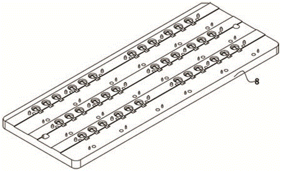
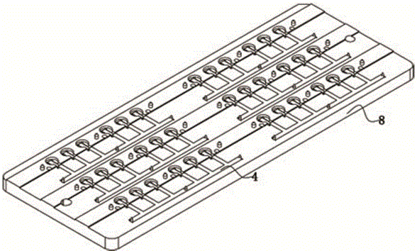
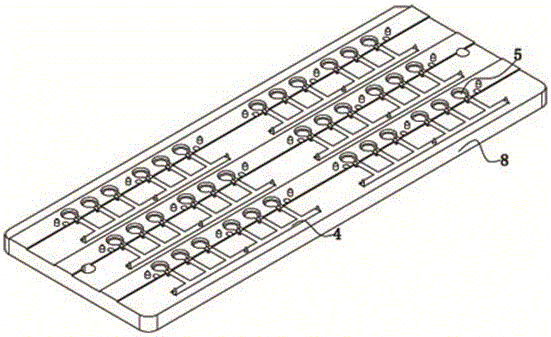
[0056] Figure 8 with Figure 18 It is a cross-sectional view of the finished product in the embodiment of the present invention. It can be clearly seen that a high-efficiency heat-conducting semiconductor chip manufacturing and packaging method includes a package shell 1, a semiconductor chip 2, a first reference electrode 3, a second reference electrode 4, a first solder sheet 5, the second soldering sheet 6, the third soldering sheet 7, the first graphite plate 8 and the second graphite plate 9, the two poles of the semiconductor chip 2 are located on the front and b...


PUM


Abstract

The invention discloses fabrication and package methods of a high-efficiency heat-conduction semiconductor chip. The high-efficiency heat-conduction semiconductor chip comprises a package shell, a semiconductor chip, a first reference electrode, a second reference electrode, a first soldering lug, a second soldering lug, a third soldering lug, a first graphite plate and a second graphite plate, wherein the semiconductor chip is laminated on a bearing surface of the first reference electrode, the back surface of the semiconductor chip is electrically connected with the bearing surface of the first reference electrode, the second reference electrode is electrically connected with a front surface of the semiconductor chip, the semiconductor chip, the first reference electrode, the second reference electrode, the first soldering lug, the second soldering lug and the third soldering lug are sealed in the package shell, and the semiconductor chip and the reference electrodes are respectively connected with the soldering lugs. With the high conductivity of the reference electrodes, high conductivity of a product is ensured; and meanwhile, with the high heat conductivity of the reference electrodes, heat energy can be rapidly transferred to a support plate, the possibility of fire and burst is reduced, and fire and burst are prevented due to the characteristic of the package shell.

Description

technical field [0001] The invention relates to the technical field of manufacturing semiconductor devices, in particular to a method for manufacturing and packaging highly efficient heat-conducting semiconductor chips. Background technique [0002] The coverage of electronic products is more and more extensive, and semiconductors are improving the development of technology in various roles. Therefore, the requirements for high-density, high-performance, high-reliability and low-cost semiconductor packaging are also more urgent. The existing heat will reduce its stable structure. However, there is also the risk of fire or explosion due to the large amount of heat that cannot be dissipated quickly. [0003] The existing pin-type semiconductor package lags behind the development goals of portable and ultra-small electronic products, and its lead inductance increases the response time of the product and reduces the protection ability of the product; when it is used with a circu...

Claims


Application Information

Patent Timeline
Patent Type & Authority Applications(China)
IPC IPC(8): H01L23/488H01L23/367H01L23/373H01L23/08H01L21/52H01L21/60
CPCH01L2224/32245H01L2224/33H01L2224/97
Inventor 周云福周湘周全
Owner BESTBRIGHT ELECTRONICS
Why Eureka
Try Eureka