Display substrate, manufacturing method thereof and transparent display device

A display substrate and substrate technology, applied in semiconductor/solid-state device manufacturing, optics, instruments, etc., can solve problems such as low cut-off, complex structure of display devices, and affecting the production efficiency of display devices

Active Publication Date: 2015-11-18
BOE TECH GRP CO LTD +1
View PDF4 Cites 5 Cited by
  • Summary
  • Abstract
  • Description
  • Claims
  • Application Information

AI Technical Summary

Problems solved by technology

The second is the filter film system formed by the Fabry-Perot interferometer. The spectral characteristics obtained by this structure are: a narrow passband can be obtained, but the cutoff band width is usually relatively narrow, and the cutoff is not deep, so the large In most cases, it is necessary to use a cut-off filter to widen the cut-off band and increase the cut-off depth. The light sheet causes the structure of the entire display device to be complex and requires more manufacturing processes, which affects the manufacturing efficiency of the display device

Method used


Image

  • Display substrate, manufacturing method thereof and transparent display device
  • Display substrate, manufacturing method thereof and transparent display device
  • Display substrate, manufacturing method thereof and transparent display device

Examples


preparation example Construction

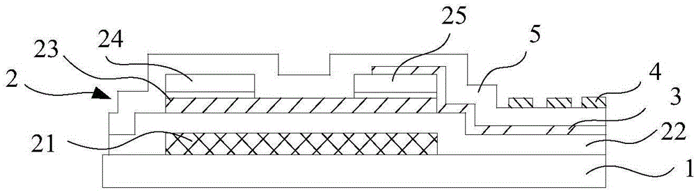
[0057] In addition, an embodiment of the present invention also provides a method for preparing a display substrate, the method including the following steps:

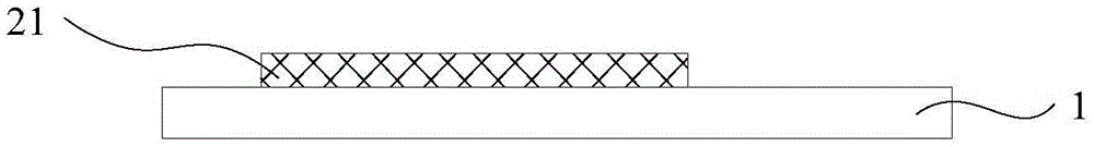
[0058] providing a substrate;

[0059] forming a first metal layer in the pixel area on the substrate;

[0060] A passivation layer is formed on the first metal layer, and the thickness of the passivation layer of multiple sub-pixel regions located in the same pixel region is different;

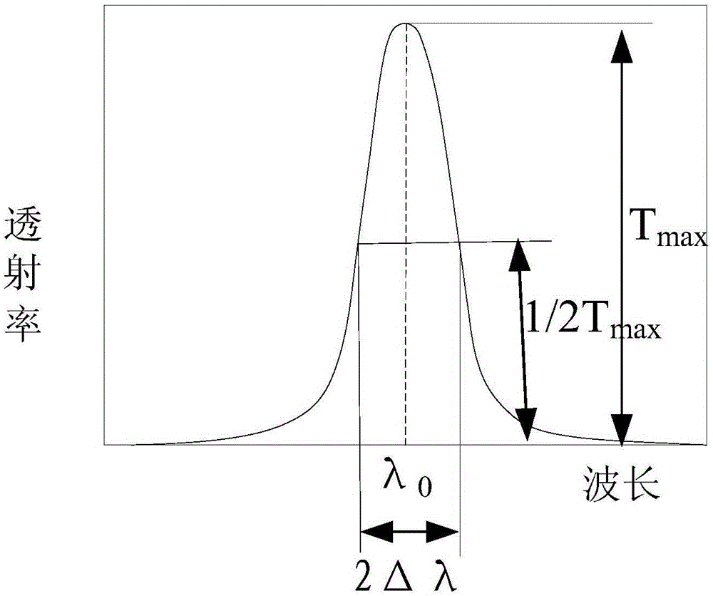
[0061] A second metal layer is formed on the passivation layer; and the first metal layer, the passivation layer and the second metal layer form a Faber cavity, and the Faber cavity allows light transmission of different wavelengths according to the thickness of the passivation layer. Pass.


PUM

PropertyMeasurementUnit
thicknessaaaaaaaaaa
thicknessaaaaaaaaaa

Abstract

The invention relates to the field of transparent display technologies, and discloses a display substrate, a manufacturing method thereof and a transparent display device. The display substrate comprises a plurality of pixel regions, wherein each pixel region comprises a plurality of sub-pixel regions; and the display substrate is characterized by further comprising a substrate body, a first metal layer, a passivation layer and a second metal layer which are sequentially arranged on the substrate body and positioned in the sub-pixel regions, wherein the first metal layer and the second metal layer are semi-transparent and semi-reflecting metal layers, and the thicknesses of the passivation layer positioned in the plurality of sub-pixel regions of the same pixel region are different; and the first metal layer, the passivation layer and the second metal layer form a Fabry-Perot cavity, and the Fabry-Perot cavity allows light with different wavelengths to pass through according to different thicknesses of the passivation layer. In the technical scheme, the display device does not need to use a color light filter when the formed Fabry-Perot cavity is adopted and can achieve the effect of selecting light rays with different colors to pass through via the display substrate, the structure of the display device is simplified, and the production efficiency is increased.

Description

technical field [0001] The invention relates to the technical field of transparent display, in particular to a display substrate, a preparation method thereof, and a transparent display device. Background technique [0002] A bandpass filter refers to a certain wavelength band, only a small section in the middle is a passband with high transmittance, and on both sides of the passband are cutoff bands with high reflectivity, such as figure 1 as shown, figure 1 The main parameters that characterize the characteristics of the filter are: [0003] lambda 0 - central wavelength or peak wavelength; [0004] T max - the transmittance at the center wavelength, i.e. the peak transmittance; [0005] 2Δλ-transmittance is half the wavelength width of the drop transmittance, that is, the half-width, or 2Δλ / λ 0 Indicates the relative half-width. [0006] Generally, the band-pass filter can have two structural forms, one is the pass band of the band-pass filter formed by the overlap...

Claims


Application Information

Patent Timeline
Patent Type & Authority Applications(China)
IPC IPC(8): H01L27/12H01L21/77
CPCG02B5/288G02B5/201H01L27/1214
Inventor 张洪术
Owner BOE TECH GRP CO LTD
Why Eureka
Try Eureka