Bidirectional meta-material absorber
A technology of absorbing body and metamaterial, applied in the field of microwave engineering technology absorbing materials, can solve the problems of reducing the absorbing rate of the absorbing body, limiting electromagnetic wave absorption, polarization insensitivity, etc.
- Summary
- Abstract
- Description
- Claims
- Application Information
AI Technical Summary
Problems solved by technology
Method used
Image
Examples
Embodiment 1
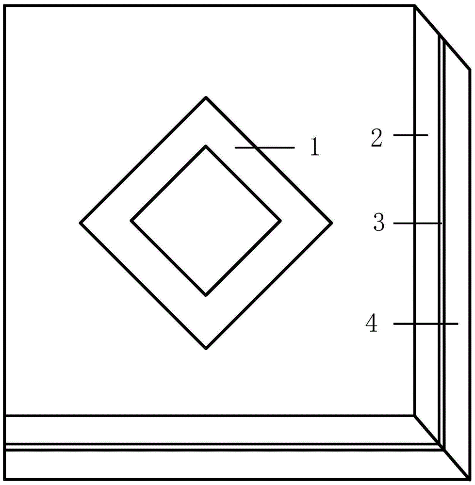
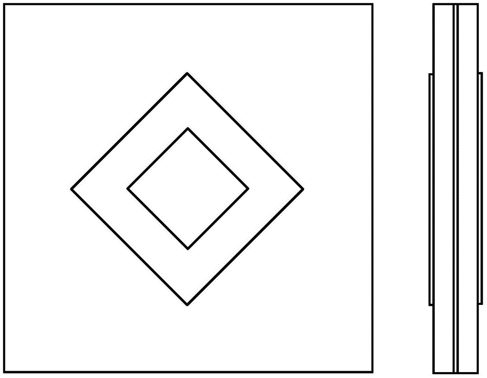
[0024] Embodiment one: below and figure 1 — Figure 8 To illustrate this embodiment, the structure of the bidirectional metamaterial absorber described in this embodiment consists of five parts: the metal thin film 3 in the middle layer, the lossy dielectric layers 2 and 4 on both sides, and the metal etched on the lossy dielectric layer Square ring 1,5. The metal thin film 3 in the middle layer is an all-metal structure without a hollow structure, and its length and width are the same as those of the lossy dielectric layers 2 and 4, and the structural properties of the two dielectric layers are the same. At the same time, the two outermost metal square rings have the same structure and size. The two metal square rings 1 and 5 are rotated by 45 degrees compared with the lossy dielectric layer, that is, the four corners of the metal square rings 1 and 5 are located on the horizontal line and the vertical line respectively, and the centers of the two metal square rings are in ...
Embodiment 2
[0025] Embodiment 2: This embodiment further limits the bidirectional metamaterial absorber described in Embodiment 1. In this embodiment, the metal film 3 in the middle layer and the metal square rings on both sides are all made of metal copper , etch on the upper and lower sides of the dielectric layers 2 and 4 by using an etching technique. The outer length of the metal square rings 1 and 5 is 4.9mm, and the inner length is 3.9mm.
Embodiment 3
[0026] Embodiment 3: This embodiment further defines the bidirectional metamaterial absorber described in Embodiment 1. In this embodiment, the dielectric layers 2 and 4 use FR4 dielectric with a dielectric constant of 4.4 and a loss of The tangent value of the angle is 0.02, and the size is 10.3mm*10.3mm*0.61mm.
[0027] Figure 4 It is the equivalent impedance of the present invention relative to free space. It can be seen from the figure that the equivalent resistance of the absorber at the absorption peak frequency point is 1, and the equivalent reactance is 0. The absorber is well realized with Impedance matching of free space.
[0028] Figure 5 — Figure 8 It is the absorption rate curve diagram of the two-way metamaterial absorber provided by the present invention according to Embodiments 1, 2, and 3. It can be seen from the figure that the two-way metamaterial absorber provided by the present invention is at a frequency of 10.18 GHz to the vertical The absorption ...
PUM
| Property | Measurement | Unit |
|---|---|---|
| Angle of rotation | aaaaa | aaaaa |
Abstract
Description
Claims
Application Information


