Voltage conversion circuit

A circuit and charge pump technology, applied in the field of circuits, can solve problems such as reducing charge pump and power consumption waste, and achieve the effect of reducing power consumption

Active Publication Date: 2015-11-18
GIGADEVICE SEMICON (BEIJING) INC
View PDF8 Cites 9 Cited by
  • Summary
  • Abstract
  • Description
  • Claims
  • Application Information

AI Technical Summary

Problems solved by technology

Charge pumps are used in some voltage conversion circuits. Usually, the clock control frequency of the charge pump is a fixed value. In order to meet the maximum load current, the clock frequency is usually designed faster, so when the load current is small, the charge pump is also It has to work at the same faster frequency, and can only rely solely on the feedback voltage of the negative feedback loop to reduce the ability of the charge pump. In this case, the ability of the charge pump to provide current is reduced, but the power consumption of the charge pump is not reduced. It causes a great waste of power consumption, so it is necessary to further improve this kind of voltage conversion circuit

Method used


Image

  • Voltage conversion circuit
  • Voltage conversion circuit
  • Voltage conversion circuit

Examples


Embodiment 1

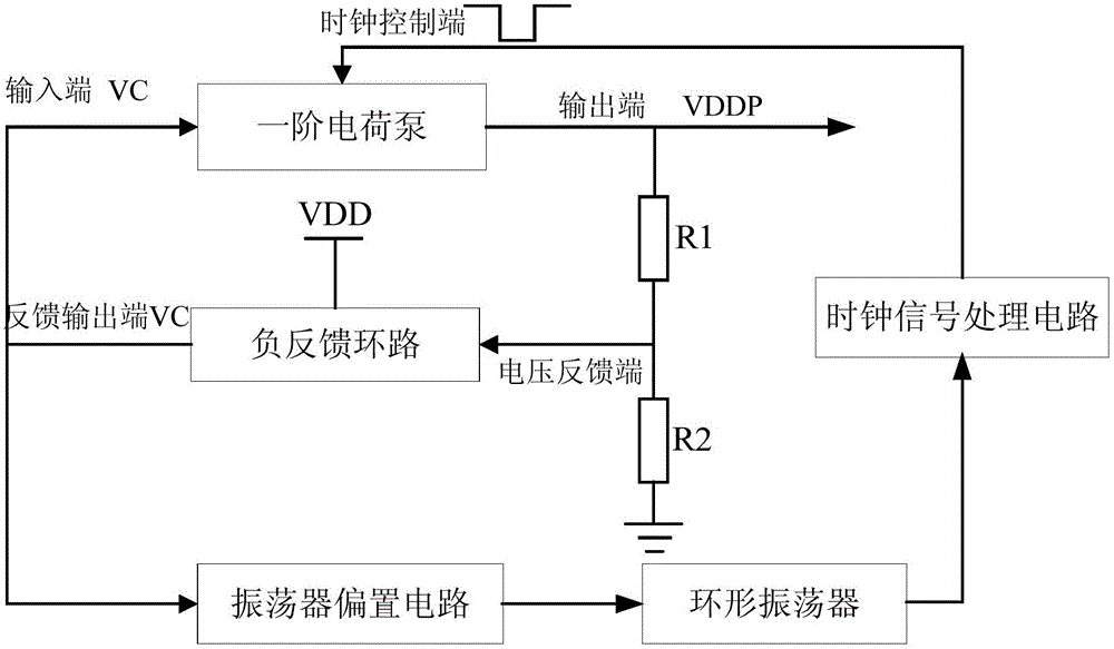
[0018] figure 1 The block diagram of a voltage conversion circuit provided by Embodiment 1 of the present invention is applicable to the case where the load requires a supply voltage with a narrow variation range. A block diagram of a voltage conversion circuit provided in this embodiment, such as figure 1 shown, including: a first-order charge pump, a negative feedback loop, an oscillator bias circuit, and a ring oscillator.

[0019] The first-order charge pump includes an input terminal, an output terminal, a forward clock control terminal (CLKB) and a reverse clock control terminal (CLK). Under the control of the clock signal, an output voltage is formed and output from the output terminal to provide voltage for the load.

[0020] The negative feedback loop includes a power supply terminal, a voltage feedback terminal and a feedback output terminal, the voltage feedback terminal is connected to the output terminal of the first-order charge pump, and is used to adjust the ...

Embodiment 2

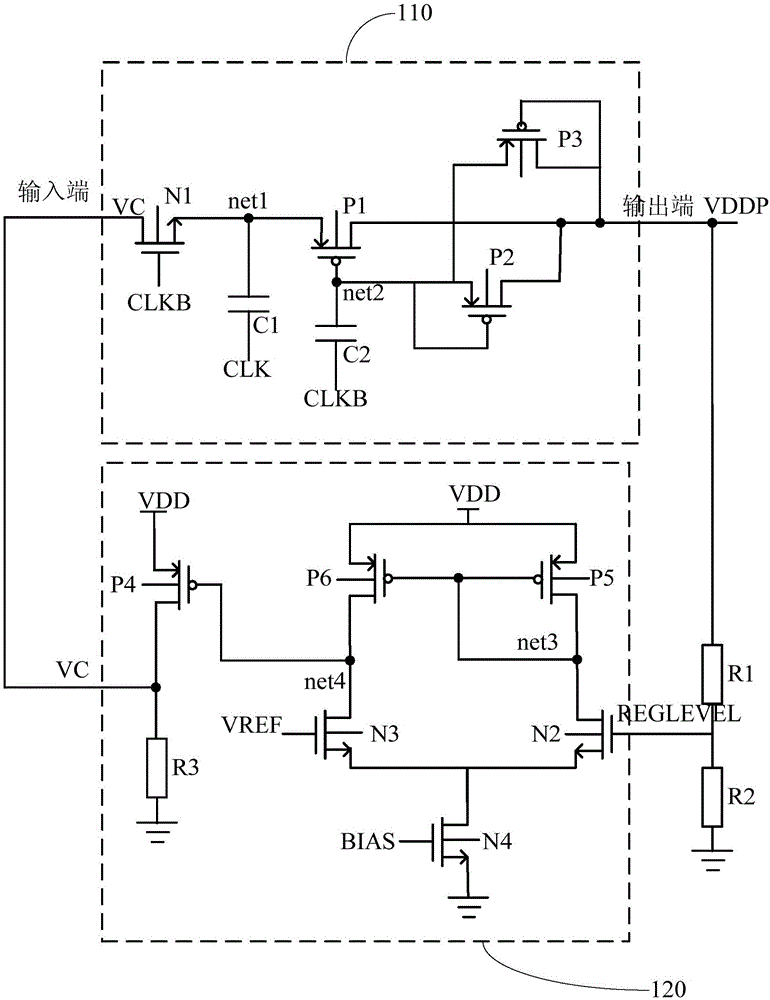
[0026] On the basis of the above embodiments, in order to more clearly describe the working principle of the first-order charge pump and the negative feedback loop, as a preferred embodiment, figure 2 The specific circuit diagram of the first-order charge pump and negative feedback loop is given, as figure 2 As shown: the first-stage charge pump 110 includes: a first N-channel metal oxide semiconductor field effect transistor (NMOS) N1, a first P-channel metal oxide semiconductor field effect transistor (PMOS) P1, a second PMOS transistor P2, third PMOS transistor P3, first capacitor C1 and second capacitor C2;

[0027] Wherein, the drain of the first NMOS transistor is the input terminal of the first-order charge pump, the gate is the positive clock control terminal, the source is connected to the reverse clock control terminal through the first capacitor, and is connected to the first PMOS The source of the tube is connected; the gate of the first PMOS tube is connected t...

Embodiment 3

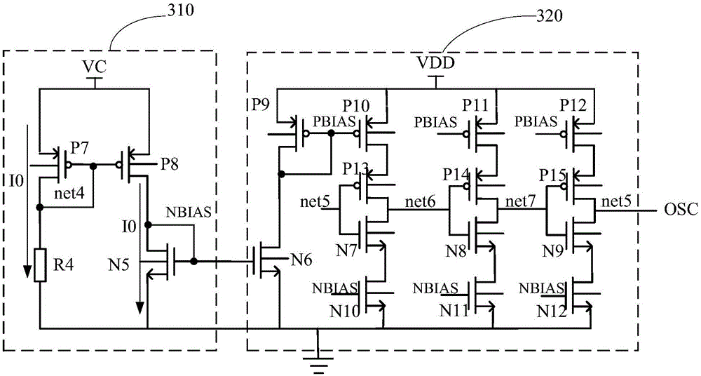
[0034] In order to realize that when the load current is small, the ability of the first-order charge pump can be reduced by the feedback voltage VC while the operating frequency of the first-order charge pump can be reduced, thereby reducing the power consumption of the first-order charge pump. This embodiment is used as a preferred embodiment. On the basis of the second embodiment, an oscillator bias circuit 310 and a ring oscillator 320 are added such as image 3 shown. The oscillator bias circuit 310 includes a seventh PMOS transistor P7, an eighth PMOS transistor P8, a fifth NMOS transistor N5 and a fourth resistor R4;

[0035] Wherein, the source of the seventh PMOS transistor is connected to the feedback voltage terminal of the negative feedback loop, the drain is grounded through the fourth resistor, and the gate is connected to the gate of the eighth PMOS transistor; The PMOS transistor is mirror-connected to the seventh PMOS transistor, and the drain is connected to...


PUM


Abstract

The invention discloses a voltage conversion circuit, which comprises a first-order charge pump, a negative feedback loop, an oscillator biasing circuit and an annular oscillator, wherein the first-order charge pump is used for forming an output voltage to be output from an output end, and providing the voltage for a load; the negative feedback loop is used for forming a feedback voltage to be output to an input end of the first-order charge pump; the oscillator biasing circuit is used for providing a biasing voltage for the annular oscillator; and the annular oscillator is used for outputting a clock signal under the control of the feedback voltage. The voltage conversion circuit controls the input voltage of the first-order charge pump and amplitude of the clock signal through the negative feedback loop, transmits the voltage at the input end of the first-order charge pump to the output end so as to form a stable output voltage, adjusting frequency of a clock control signal of the first-order charge pump through the annular oscillator according to load current condition, and reduces power consumption of the system under the condition of guaranteeing that the stable target voltage is output.

Description

technical field [0001] Embodiments of the present invention relate to circuit technology, and in particular to a voltage conversion circuit. Background technique [0002] Voltage conversion circuits are used to convert the voltage of a signal from one analog voltage range to another analog voltage range. Charge pumps are used in some voltage conversion circuits. Usually, the clock control frequency of the charge pump is a fixed value. In order to meet the maximum load current, the clock frequency is usually designed faster, so when the load current is small, the charge pump is also It has to work at the same faster frequency, and can only rely solely on the feedback voltage of the negative feedback loop to reduce the ability of the charge pump. In this case, the ability of the charge pump to provide current is reduced, but the power consumption of the charge pump is not reduced. This causes a great waste of power consumption, so further improvement of this type of voltage c...

Claims


Application Information

Patent Timeline
Patent Type & Authority Applications(China)
IPC IPC(8): H02M3/07
Inventor 陈晓璐胡洪
Owner GIGADEVICE SEMICON (BEIJING) INC
Why Eureka
Try Eureka