

A test probe and test device
A technology for testing probes and test terminals, which is applied in the direction of measuring devices, measuring electricity, and measuring electrical variables. It can solve problems such as test result errors, sample surface scratches and damage, and test probe wear, so as to achieve reduced friction, good contact, The effect of reducing scratch damage as well as
- Summary
- Abstract
- Description
- Claims
- Application Information
AI Technical Summary
Problems solved by technology
Method used
Image

Examples
Embodiment Construction
[0049] The following will clearly and completely describe the technical solutions in the embodiments of the present invention with reference to the accompanying drawings in the embodiments of the present invention. Obviously, the described embodiments are only some, not all, embodiments of the present invention. Based on the embodiments of the present invention, all other embodiments obtained by persons of ordinary skill in the art without making creative efforts belong to the protection scope of the present invention.
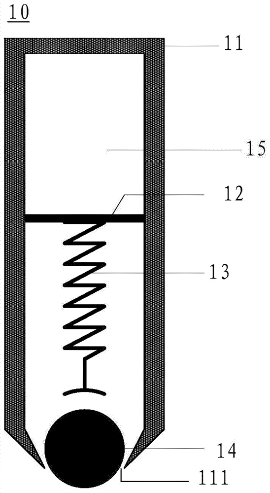
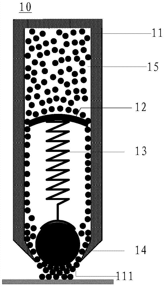
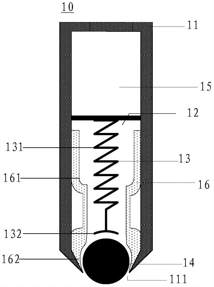
[0050] Embodiments of the present invention provide a test probe, specifically, refer to figure 1 , 2 As shown, among them, figure 2 for figure 1 The schematic structure diagram of the test probe in working state is shown. The test probe 10 includes: a housing 11 and a piston 12, an elastic device 13 and a ball 14 arranged inside the housing;
[0051] The housing 11 includes a test end and a fixed end, and the test end is provided with a test opening 111;...
PUM
 Abstract
Description
Claims
Application Information