

SRAM (static random access memory) storage unit, SRAM memory and control method therefor
A memory unit and memory technology, applied in static memory, digital memory information, information storage, etc., can solve the problems of increasing the size of the memory cell array, increasing the number of transistors, unfavorable integrated circuit integration and chip size miniaturization, etc., and achieve bit line Effect of small cell size and improved stability
- Summary
- Abstract
- Description
- Claims
- Application Information
AI Technical Summary
Problems solved by technology
Method used
Image


Examples
Embodiment 1
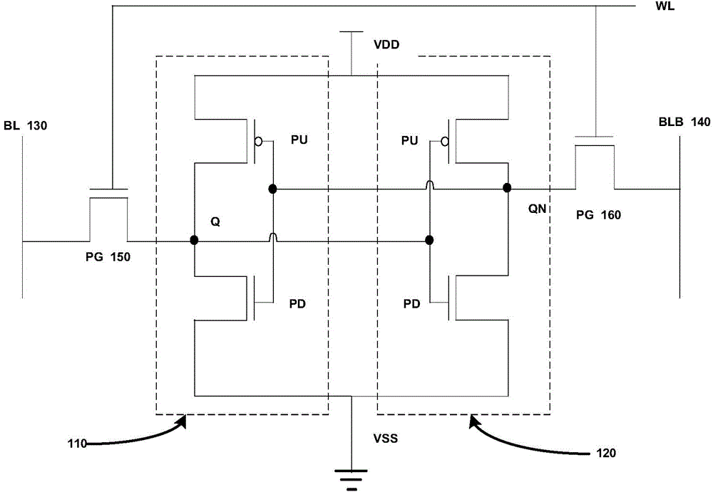
[0036] According to one aspect of the present invention, the present invention provides a kind of SRAM memory cell comprising: word line pair, and described word line pair comprises write word line 380 and read word line 370; Bit line pair, described bit line pair comprises write position line 330 and read bit line 340;
[0037] a memory cell located between the pair of word lines and the pair of bit lines, the memory cell includes a read end and a write end;
[0038] The read transfer transistor 360 at the read end is controlled by the read word line 370 to realize information reading, and the write transfer transistor 350 at the write end is controlled by the write word line 380 to realize information input.
[0039] Specifically, the size of the storage unit largely determines the size of the SRAM chip, therefore, it is necessary to make the size of the storage unit as small as possible. The memory cell may be constituted by an inversion cell for inverting the potential of...
Embodiment 2
[0051] The present invention also provides an SRAM memory, the SRAM memory includes the SRAM storage unit described in Embodiment 1, wherein the memory may include several SRAM storage units, wherein the SRAM storage unit may be arranged along a row oriented or otherwise arranged.
[0052] The present invention also provides a control method of the SRAM memory, the control method comprising:
[0053] When performing a write operation on the selected one of the memory cells, the write word line corresponding to the selected one is set to a high potential, and the information transmitted by the peripheral circuit to the pair of bit lines is used as input; and
[0054] When performing a read operation on a selected one of the plurality of memory cells, the read word line corresponding to the selected one is set to a low potential, the read bit line is set to a high potential, and the unselected one is set to a high potential. The read word line corresponding to one of them is se...
PUM
 Abstract
Description
Claims
Application Information