Method for improving evenness of critical size

A technology of critical dimension and uniformity, applied in the field of semiconductor manufacturing, can solve the problems of poor mirror image of exposure system, affecting the uniformity of critical dimensions of through holes, unevenness of the central area and edge area of ​​the wafer, etc., so as to improve uniformity and reduce RC parameters. Abnormal times, the effect of improving product yield

Inactive Publication Date: 2015-11-25
SEMICON MFG INT (SHANGHAI) CORP
View PDF9 Cites 7 Cited by
  • Summary
  • Abstract
  • Description
  • Claims
  • Application Information

AI Technical Summary

Problems solved by technology

Through physical failure analysis (PFA), it is found that the reason is that when the photolithographic pattern is formed, the critical dimension of the via pattern on the edge of the wafer is small, and some vias are not opened during the subsequent etching process, resulting in logic errors in the device
[0004] The reasons for the unevenness of the key dimensions are mainly as follows: 1. In the CMP (Chemical Mechanical Planarization) process, the central area and the edge area of ​​the wafer are not flat, and there is a certain height difference, which will cause the central area after exposure. Non-uniform critical dimensions with edge regions
2. Problems in the exposure system, such as bending of the mirror field and poor mirror ...

Method used


Image

  • Method for improving evenness of critical size
  • Method for improving evenness of critical size
  • Method for improving evenness of critical size

Examples


Embodiment Construction

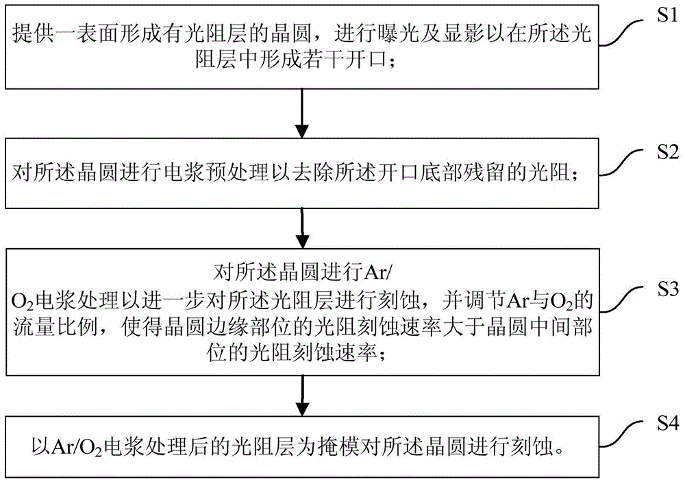
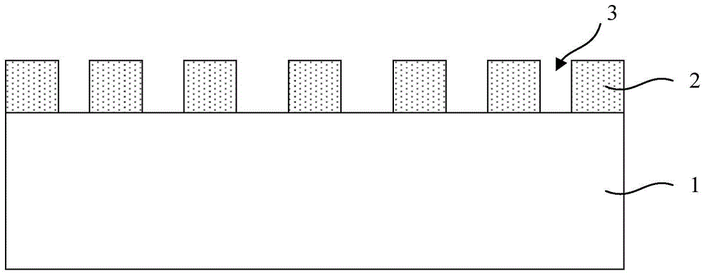
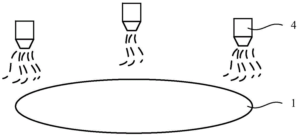
[0037] Embodiments of the present invention are described below through specific examples, and those skilled in the art can easily understand other advantages and effects of the present invention from the content disclosed in this specification. The present invention can also be implemented or applied through other different specific implementation modes, and various modifications or changes can be made to the details in this specification based on different viewpoints and applications without departing from the spirit of the present invention.

[0038] see Figure 1 to Figure 8 . It should be noted that the diagrams provided in this embodiment are only schematically illustrating the basic idea of ​​the present invention, and only the components related to the present invention are shown in the diagrams rather than the number, shape and shape of the components in actual implementation. Dimensional drawing, the type, quantity and proportion of each component can be changed arb...


PUM


Abstract

The present invention provides a method for improving an evenness of a critical size, including at least the steps as follows: S1: providing a wafer, wherein, the wafer has a photoresist layer formed on a surface of the wafer for exposing, developing and forming a plurality of openings in the photoresist layer; S2. performing a plasma pre-treatment to the wafer for removing residual photoresistances on the bottoms of the openings; S3. performing a Ar/O2 plasma treatment to the wafer for further etching the photoresist layer, and adjusting a flow proportion of Ar and O2 so that an etching rate of the photoresist on the edge part of the wafer is larger than an etching rate of the photoresist on the middle part of the wafer; S4. and etching the wafer by utilizing the photoresist after Ar/O2 plasma treatment as a masking film. The method further includes the step of Ar/O2 plasma treatment after the step of plasma pre-treatment, the etching rate of the photoresist on the edge part of the wafer is larger than the etching rate of the middle part of the wafer by the adjustment of the flow proportion of Ar and O2, and thereby adjusting the opening size of the photoresists on the edge part of the wafer and the middle part of the wafer so as to improve the evenness of the critical size of an etched through hole.

Description

technical field [0001] The invention belongs to the field of semiconductor manufacturing and relates to a method for improving the uniformity of critical dimensions. Background technique [0002] Semiconductor technology continues to move towards smaller process nodes driven by Moore's Law. With the continuous advancement of semiconductor technology, the functions of devices are becoming more and more powerful, but the difficulty of semiconductor manufacturing is also increasing day by day. Photolithography is the most critical production technology in the semiconductor manufacturing process. In the formation of lithographic patterns, it is a great challenge to control the line width of lithographically defined lines, because the line width of the lines will affect the final critical dimension. Non-uniformity in critical dimensions degrades device yield. As critical dimensions decrease, control of critical dimension uniformity becomes more important. [0003] In the manu...

Claims


Application Information

Patent Timeline
IPC IPC(8): H01L21/027H01L21/768
Inventor 孙超李斌生张英男丁超钟鑫生
Owner SEMICON MFG INT (SHANGHAI) CORP
Why Eureka
Try Eureka