Device of three-dimensional integrated circuit and fabrication method of device

A technology of integrated circuits and circuit components, which is applied in the field of three-dimensional integrated circuit devices and its preparation, and can solve the problem that the capacity and internal resistance of capacitors to store electric energy, and the energy transmission indicators of inductances cannot meet the production requirements of devices, and the area of ​​inductance and capacitance is limited. And other issues

Active Publication Date: 2015-11-25
WUHAN XINXIN SEMICON MFG CO LTD
View PDF4 Cites 2 Cited by
  • Summary
  • Abstract
  • Description
  • Claims
  • Application Information

AI Technical Summary

Problems solved by technology

[0006] In view of the above problems, the present invention provides a three-dimensional integrated circuit device and its preparation method to solve the problem that the area of ​​the inductance and capacitance in the prior art is limited, resulting in the capacity of the capacitor to store electric energy, the internal resistance and the energy transmission index of the inductance not reaching the device. deficiencies in production requirements

Method used


Image

  • Device of three-dimensional integrated circuit and fabrication method of device
  • Device of three-dimensional integrated circuit and fabrication method of device
  • Device of three-dimensional integrated circuit and fabrication method of device

Examples


Embodiment Construction
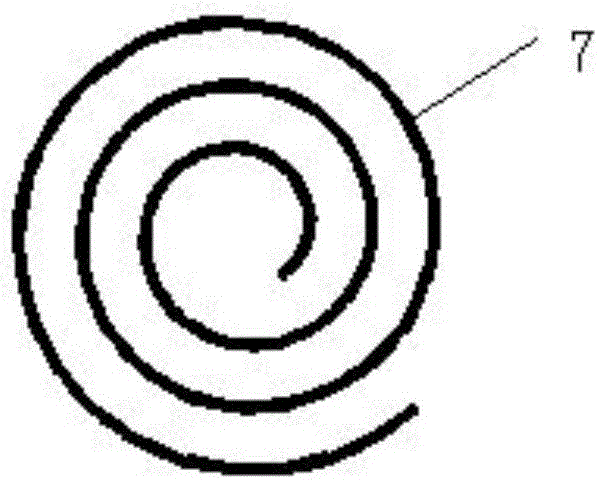
[0054] The core idea of ​​the present invention is to arrange circuit elements on the backside of the non-device area.

[0055] The present invention will be further described below in conjunction with the accompanying drawings and specific embodiments, but not as a limitation of the present invention.

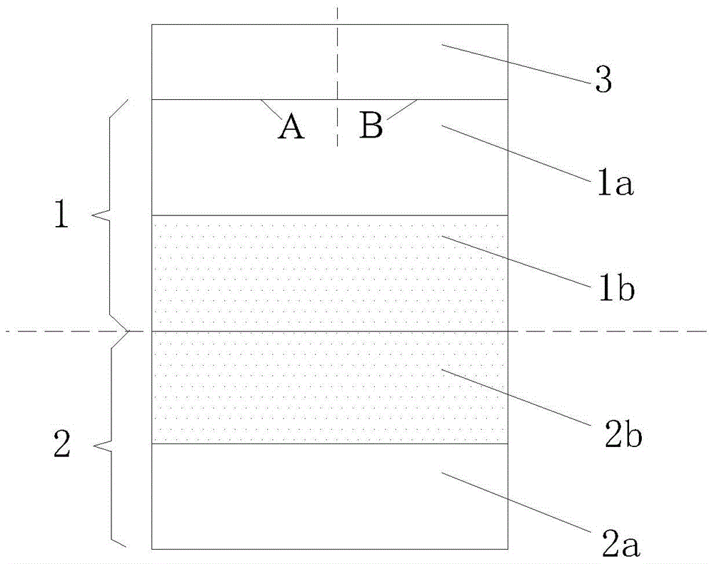
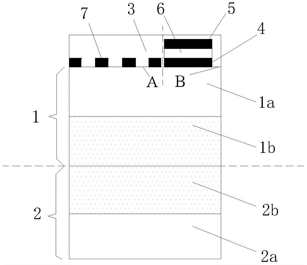
[0056] Such as figure 1As shown, the bonded wafer specifically includes a first wafer 1 and a second wafer 2, the first wafer 1 is located above the second wafer 2, and the front surfaces of the two wafers are bonded to each other, which can be based on It is conventional in this field to set the front and back sides of the above-mentioned first wafer 1 and second wafer 2, such as according to the position of the device structure formed in the wafer, set the side on which the device is provided as the front side of the wafer, correspondingly If so, the other side of the wafer opposite to the front side is used as the back side, thereby forming the front side and the back side...


PUM


Abstract

The invention relates to the technical field of fabrication of a semiconductor, in particular to a device of a three-dimensional integrated circuit and a fabrication method of the device. By arranging a circuit component with an inductor capacitor on the surface of the back side of a wafer in a non-device region, the inductor capacitor contacts a large part of the area of the back side of the wafer, therefore, the area of the fabricated inductor capacitor is relatively large, and indexes such the capacity for storing electric energy, internal resistance and the like of the capacitor and the energy transmission index of the inductor can reach the requirement for device production; and meanwhile, the back side of the wafer can be used for forming a leading line, and thus, the large-area capacitor cannot affect the design and the distribution of other circuit components.

Description

technical field [0001] The invention relates to the technical field of semiconductor manufacturing, in particular to a three-dimensional integrated circuit device and a preparation method thereof. Background technique [0002] Inductors and capacitors are the most basic and important electronic components in electronic equipment, and are currently widely used in important fields such as computers, communications, transportation, and aviation. In electronic equipment with timing, filtering, and coupling devices, capacitors can store and intensify electrical energy, while inductance, as one of the properties of electronic circuits, has also received increasing attention in filtering, oscillating, and delaying circuits. [0003] With the advancement of science and technology and the improvement of social informatization, in the semiconductor integrated circuit design process, it is often accompanied by complex electronic components such as inductors and capacitors. For example,...

Claims


Application Information

Patent Timeline
Patent Type & Authority Applications(China)
IPC IPC(8): H01L23/522H01L23/64H01L21/02
Inventor 朱继锋梅绍宁鞠韶复
Owner WUHAN XINXIN SEMICON MFG CO LTD
Why Eureka
Try Eureka