Composite structure and fabrication method of magnetic field regulating LED luminous brightness

A composite structure, luminous brightness technology, applied in the direction of electrical components, circuits, semiconductor devices, etc., can solve the problems of reducing luminous efficiency, red shift, etc., and achieve the effect of low material purity requirements, high mechanical strength, and broad market application prospects

Active Publication Date: 2018-01-26
BEIJING INST OF NANOENERGY & NANOSYST
View PDF2 Cites 0 Cited by
  • Summary
  • Abstract
  • Description
  • Claims
  • Application Information

AI Technical Summary

Problems solved by technology

In general, there is a strong polarization effect in the wurtzite-based GaN-based or ZnO-based LED stacked thin film materials, and the built-in electric field generated by the polarization effect will bend and tilt the energy band, and electrons and holes will be separated in space. Separation reduces the luminous efficiency of the LED, and at the same time, the luminous wavelength will also be found to be red-shifted

Method used


Image

  • Composite structure and fabrication method of magnetic field regulating LED luminous brightness
  • Composite structure and fabrication method of magnetic field regulating LED luminous brightness
  • Composite structure and fabrication method of magnetic field regulating LED luminous brightness

Examples


Embodiment 1

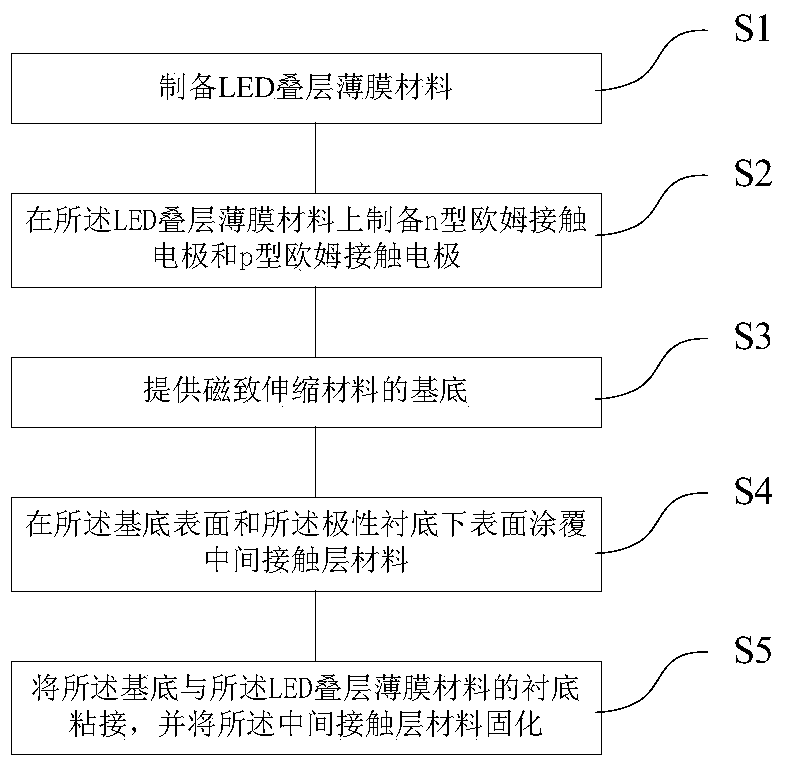
[0063] according to figure 2 The flow chart shown is to make a composite structure that regulates the luminance of blue LEDs by a magnetic field, and the following steps are performed in sequence:

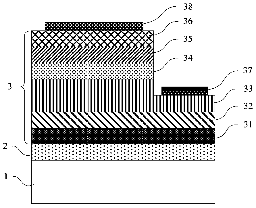
[0064] (a) Epitaxially grow a 2 μm thick GaN buffer layer and a 3 μm thick n-type GaN conductive layer (doped with Si, n-type doping concentration of 3*10 18 / cm 3 ), five 2nm thick In 0.15 Ga 0.85 N / 15nm thick GaN quantum well strained active region, 50nm thick p-type Al 0.1 Ga 0.9 N electron blocking layer and 100nm thick p-type GaN conductive layer to obtain blue LED stacked thin film material;

[0065] (b) using micromachining photolithography means to make mesa etching patterns on the blue LED laminated film material substrate;

[0066] Carrying out dry etching on the patterned blue LED stacked film material substrate, the etching depth reaches the n-GaN conductive layer, and the n-GaN conductive layer is etched by 500nm to form an etching mesa;

[0067] Fabricate n-Ga...

Embodiment 2

[0072] according to figure 2 The flow chart shown is to make a composite structure that regulates the luminance of green LEDs by a magnetic field, and the following steps are performed in sequence:

[0073] (a) Epitaxial growth of 2 μm thick GaN buffer layer and 3 μm thick n-type GaN conductive layer (doped with Si, n-type doping concentration of 3*10 18 / cm 3 ), seven 2nm thick In 0.3 Ga 0.7 N / 12nm thick GaN quantum well strained active region, 50nm thick p-type Al 0.05 Ga 0.95 N electron blocking layer and 100nm thick p-type GaN conductive layer to obtain green LED laminated film material;

[0074] (b) using micromachining photolithography means to make mesa etching patterns on the green LED laminated film material substrate; dry etching the patterned green LED laminated film material substrate, engraving The etching depth reaches the n-GaN conductive layer, and the n-GaN conductive layer is etched by 500nm to form an etching mesa; n-GaN ohmic contact electrodes Ti / Al...


PUM

PropertyMeasurementUnit
thicknessaaaaaaaaaa
thicknessaaaaaaaaaa
thicknessaaaaaaaaaa

Abstract

The invention relates to a composite structure and a manufacturing method for regulating the luminance of LEDs by a magnetic field. The composite structure is composed of a magnetostrictive material substrate and an LED laminated film material. A unified whole is formed, wherein the LED stacked film materials are polar substrate, buffer layer, n-type conductive layer, strained active region, p-type electron blocking layer and p-type conductive layer in sequence. Under the action of an external magnetic field, the luminous efficiency of the strained active region in the LED laminated film material is regulated through the stress / strain of the magnetostrictive material substrate, thereby realizing the function of continuously adjustable LED luminous brightness. The composite structure proposed by the present invention is novel, and the manufacturing method is simple and easy, which is conducive to the integration of new magnetic-force-electric-optical devices and systems, and will be applied to adjustable light display, magnetic sensing imaging, self-driven sensor network, magnetic electro-optic integrated systems, etc.

Description

technical field [0001] The invention relates to the field of semiconductor optoelectronic devices, in particular to a magnetic field control LED emitter [0002] The composite structure and the manufacturing method of the luminance aim at realizing the continuous adjustment of the luminance of the LED. Background technique [0003] The new semiconductor LED solid-state lighting is one of the most promising new technologies in the 21st century, and will become another leap in the history of human lighting after incandescent lamps and fluorescent lamps. As the third-generation semiconductor materials, both GaN-based and ZnO-based material systems have large band gaps. The former can be continuously adjusted from 0.7eV to 6.2eV, and the latter can be continuously adjusted from 2.3eV to 10.8eV. Light display in the full spectrum range from infrared to ultraviolet, and GaN-based LEDs have achieved remarkable results in blue-green light display, green solid-state lighting, landsc...

Claims


Application Information

Patent Timeline
Patent Type & Authority Patents(China)
IPC IPC(8): H01L33/00
Inventor 翟俊宜彭铭曾
Owner BEIJING INST OF NANOENERGY & NANOSYST
Why Eureka
Try Eureka