Package structure and package method of organic light-emitting diode (OLED) device

A technology of packaging structure and packaging method, which is applied to the manufacturing of electric solid-state devices, semiconductor devices, semiconductor/solid-state devices, etc., can solve problems such as the deterioration of packaging structure performance, and achieve the effect of improving packaging effect, simple method, and enhancing the ability to prevent water vapor.

Inactive Publication Date: 2015-11-25
TCL CHINA STAR OPTOELECTRONICS TECH CO LTD
View PDF7 Cites 36 Cited by
  • Summary
  • Abstract
  • Description
  • Claims
  • Application Information

AI Technical Summary

Problems solved by technology

However, the encapsulation structure of this kind of OLED device depends heavily on the quality of each film layer, especially the quality of the inorganic film layer, such as figure 2 As shown, the inevitable defects of the inorganic film formed at low temperature will form water vapor erosion channels, which will cause the performance of the packaging structure to deteriorate.

Method used


Image

  • Package structure and package method of organic light-emitting diode (OLED) device
  • Package structure and package method of organic light-emitting diode (OLED) device
  • Package structure and package method of organic light-emitting diode (OLED) device

Examples


Embodiment Construction

[0034] In order to further illustrate the technical means adopted by the present invention and its effects, the following describes in detail in conjunction with preferred embodiments of the present invention and accompanying drawings.

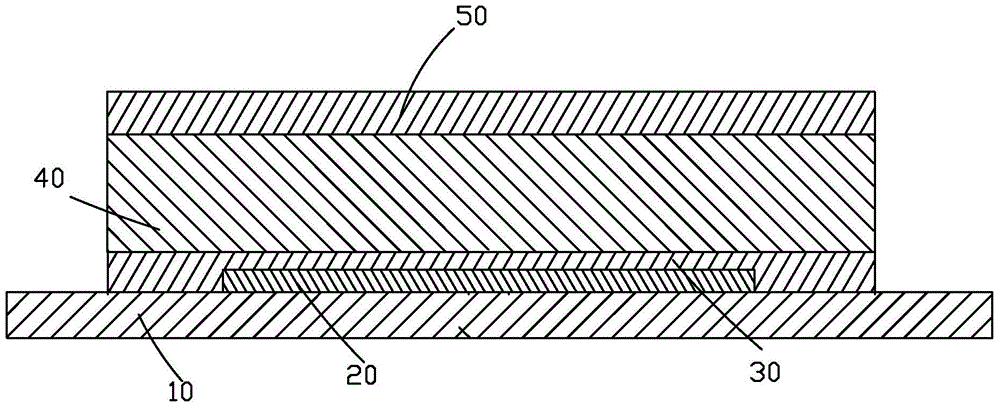
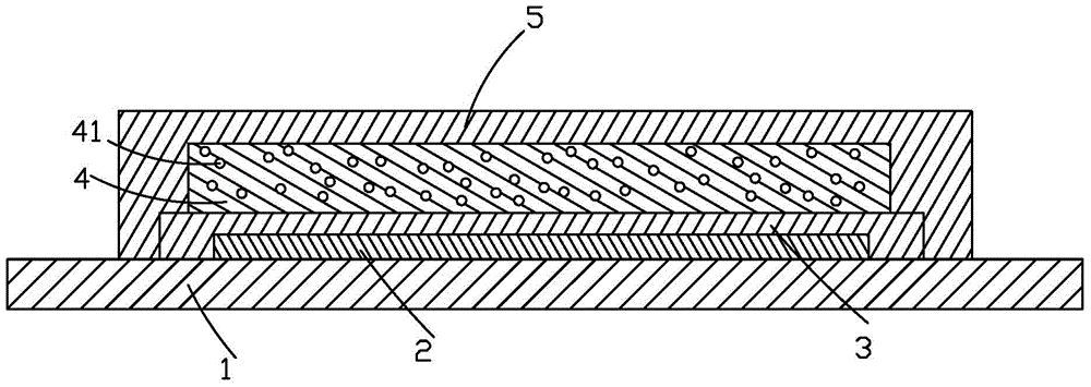
[0035] see image 3 , the present invention provides a packaging structure of an OLED device, comprising a substrate 1, an OLED device 2 disposed on the substrate 1, a first barrier layer 3 formed on the OLED device 2, a first barrier layer 3 formed on the first barrier A buffer layer 4 on the layer 3, a second barrier layer 5 formed on the buffer layer 4;

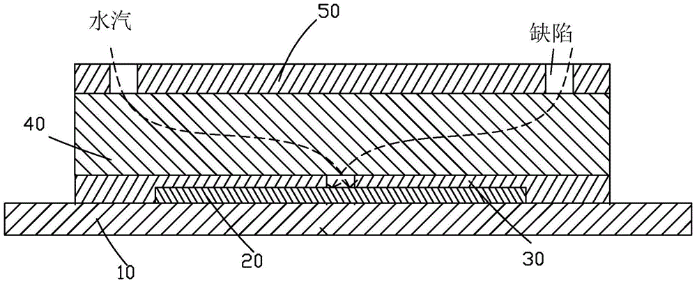
[0036] The buffer layer 4 is mixed with water-absorbing material particles 41; Figure 4 As shown, when the first barrier layer 3 or the second barrier layer 5 has defects, the water-absorbing material particles 41 in the buffer layer 4 can absorb water vapor, thereby enhancing the ability of the packaging structure to block water vapor, and then Effectively prolong the life of OLED devi...


PUM


Abstract

The invention provides a package structure and a package method of an organic light-emitting diode (OLED) device. The package structure of the OLED device comprises a substrate (1), an OLED device (2), a first blocking layer (3), a buffer layer (4) and a second blocking layer (5), wherein the OLED device (2) is arranged on the substrate (1), the first blocking layer (3) is formed on the OLED device (2), the buffer layer (4) is formed on the first blocking layer (3), the second blocking layer (5) is formed on the buffer layer (4), and the buffer layer (4) is doped with water absorption particles (41). By doping the water absorption particles into the buffer layer, the ability of preventing moisture of the package structure is enhanced, and thus, the service life of the OLED device can be effectively prolonged. According to the package method of the OLED device, moisture invasion can be effectively blocked, the package effect is improved, and the service life of the OLED is effectively prolonged. The method is simple and is high in operability.

Description

technical field [0001] The invention relates to the field of packaging technology, in particular to a packaging structure of an OLED device and a packaging method thereof. Background technique [0002] OLED is Organic Light-Emitting Diode (Organic Light-Emitting Diode), which has the characteristics of self-illumination, high brightness, wide viewing angle, high contrast, flexibility, and low energy consumption. Instead of traditional liquid crystal displays, it is widely used in mobile phone screens, computer monitors, full-color TVs, etc. Unlike traditional liquid crystal display technology, OLED display technology does not require a backlight, and uses very thin coatings of organic materials and glass substrates that emit light when an electric current passes through them. However, because organic materials are easy to react with water vapor or oxygen, as a display device based on organic materials, OLED displays have very high requirements for packaging. [0003] Most ...

Claims


Application Information

Patent Timeline
Patent Type & Authority Applications(China)
IPC IPC(8): H01L51/52H01L51/56
CPCH10K50/846H10K50/844H10K50/80H10K71/00
Inventor 钱佳佳
Owner TCL CHINA STAR OPTOELECTRONICS TECH CO LTD
Why Eureka
Try Eureka