Liquid crystal display panel, array substrate and manufacturing method of array substrate

An array substrate and substrate technology, applied in the field of liquid crystal display, can solve the problems of increasing the black matrix and reducing the pixel aperture ratio, and achieve the effect of increasing the pixel aperture ratio, reducing the size, and reducing the resistance

Active Publication Date: 2015-12-02
TCL CHINA STAR OPTOELECTRONICS TECH CO LTD
View PDF6 Cites 19 Cited by
  • Summary
  • Abstract
  • Description
  • Claims
  • Application Information

AI Technical Summary

Problems solved by technology

However, due to the need to avoid the short circuit between the floating electrode layer 14 and the common electrode layer 15, it is necessary to increase the edge distance between the common electrode layer 15 and the floating electrode layer 14, which will undoubtedly increase the size of the black matrix (BlackMatrix, BM) layer 16, thereby reducing the pixel aperture ratio

Method used


Image

  • Liquid crystal display panel, array substrate and manufacturing method of array substrate
  • Liquid crystal display panel, array substrate and manufacturing method of array substrate
  • Liquid crystal display panel, array substrate and manufacturing method of array substrate

Examples


Embodiment Construction

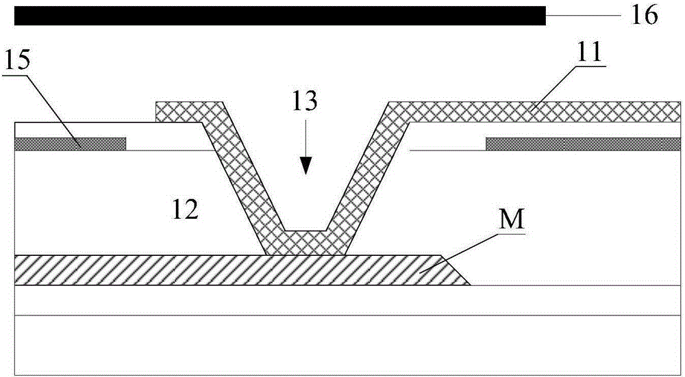
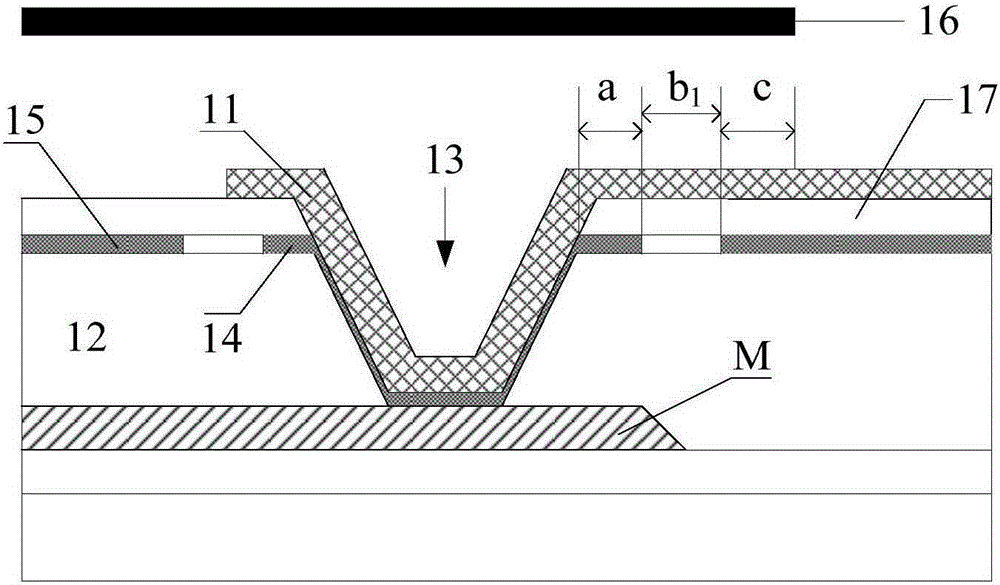
[0021] The following will clearly and completely describe the technical solutions of the exemplary embodiments provided by the present invention with reference to the accompanying drawings in the embodiments of the present invention.

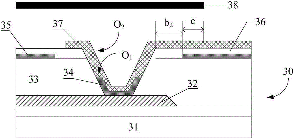
[0022] image 3 is a structural cross-sectional view of an embodiment of the array substrate of the present invention. Such as image 3 As shown, the array substrate 30 includes a substrate 31 , a metal layer 32 , a first passivation layer 33 , a floating electrode layer 34 , a common electrode layer 35 , a second passivation layer 36 and a pixel electrode layer 37 .

[0023] Wherein, the metal layer 32 is formed on the substrate 31; the first passivation layer 33 is formed on the metal layer 32 and is formed with a first contact hole O that exposes the surface of the metal layer 32 1 ; The floating electrode layer 34 covers the first contact hole O 1 The bottom surface of and the first contact hole O connected to the bottom surface 1 A part...


PUM

PropertyMeasurementUnit
thicknessaaaaaaaaaa
thicknessaaaaaaaaaa

Abstract

The invention provides an array substrate. A floating electrode layer is additionally arranged in a contact hole enabling electric connection of a TFT metal layer and a pixel electrode layer to be achieved, so that the pixel electrode layer is electrically connected with the metal layer again through the bridging of the floating electrode layer. Resistance at the contact hole and the film breakage probability of the pixel electrode layer in the contact hole can be reduced. In addition, the edge of the floating electrode layer is located in the contact hole, the dimension of a corresponding black matrix layer can be reduced, and the pixel aperture opening ratio can be increased. The invention further provides a method for manufacturing the array substrate and a liquid crystal display panel with the array substrate.

Description

technical field [0001] The invention relates to the technical field of liquid crystal display, in particular to an array substrate, a manufacturing method thereof, and a liquid crystal display panel having the array substrate. Background technique [0002] Such as figure 1 In the illustrated pixel structure of the array substrate, the pixel electrode layer 11 needs to be electrically connected to the metal layer M of the TFT (ThinFilm Transistor, thin film transistor) through the contact hole (Via) 13 formed in the passivation layer 12 . But the thickness of the pixel electrode layer 11 is 40-60 nanometers, the thickness of the passivation layer 12 is 1.5-3 microns, and the opening of the contact hole 13 is relatively small, which makes the disconnection of the pixel electrode layer 11 formed in the contact hole 13 The higher probability of the film or the smaller thickness will result in higher resistance at the contact hole 13 and affect the display quality. In order to ...

Claims


Application Information

Patent Timeline
Patent Type & Authority Applications(China)
IPC IPC(8): G02F1/1362H01L27/12H01L21/77
CPCG02F1/136227H01L27/1214H01L27/1259G02F1/133512G02F2201/40G02F1/133345G02F1/133514G02F1/134309G02F1/13439G02F1/1368G02F2201/121G02F2201/123
Inventor 王勐
Owner TCL CHINA STAR OPTOELECTRONICS TECH CO LTD
Why Eureka
Try Eureka