Embedded touch array substrate, display panel and production method

An array substrate, embedded technology, used in semiconductor/solid-state device manufacturing, optics, instruments, etc., can solve the problems of complex process and high cost, and achieve the effect of simplifying the process, reducing the cost, and reducing the probability of film breakage

Inactive Publication Date: 2018-09-07
WUHAN CHINA STAR OPTOELECTRONICS TECH CO LTD
View PDF8 Cites 13 Cited by
  • Summary
  • Abstract
  • Description
  • Claims
  • Application Information

AI Technical Summary

Problems solved by technology

[0020] A total of 14 photomask processes are required to complete, the process is complex and the cost is high

Method used


Image

  • Embedded touch array substrate, display panel and production method
  • Embedded touch array substrate, display panel and production method

Examples


Embodiment Construction

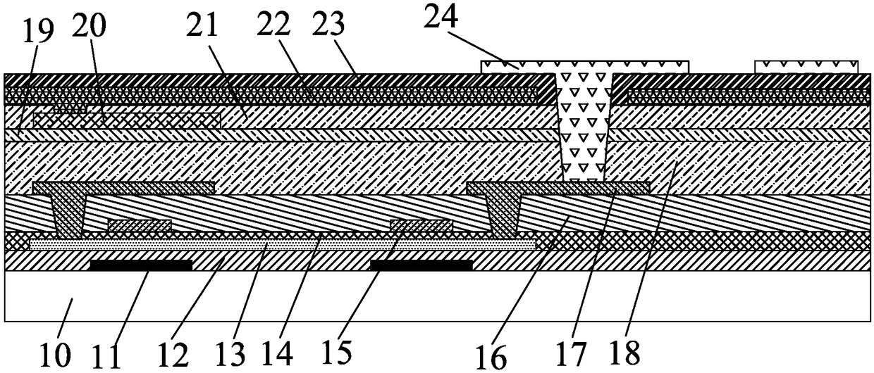
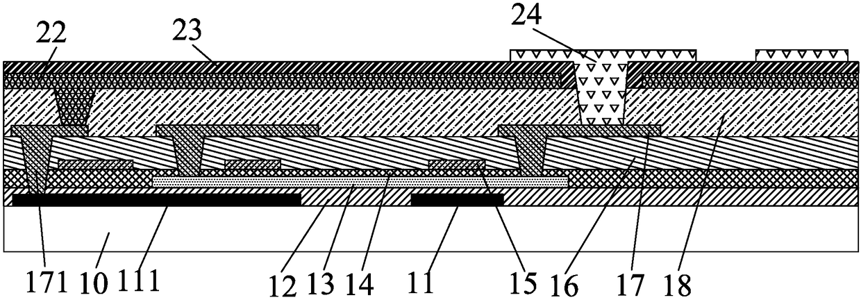
[0064] see figure 2 , which is a schematic cross-sectional expanded view of a preferred embodiment of the in-cell touch array substrate of the present invention. The embedded touch array substrate of this preferred embodiment mainly includes: a substrate 10; a low temperature polysilicon thin film transistor array disposed on the substrate 10, the low temperature polysilicon thin film transistor array includes a patterned light-shielding layer 11 and a patterned source and drain Pole layer 17; a patterned flat layer 18 arranged on the low-temperature polysilicon thin film transistor array; a patterned bottom transparent electrode 22 arranged on the flat layer 18, which can be used as a touch signal electrode; arranged on the bottom transparent electrode 22 A patterned passivation layer 23; a patterned top transparent electrode 24 disposed on the passivation layer 23, which can be used as a pixel electrode;

[0065] In the present invention, the source and drain layer 17 meta...


PUM


Abstract

The invention relates to an embedded touch array substrate, a display panel and a production method. The embedded touch array substrate comprises a substrate (10); a low temperature polycrystalline silicon thin film transistor array which is set on the substrate (10) and comprises patterned light shielding layers (11) and patterned source and drain layers (17); a patterned flat layer (18) set on the low temperature polycrystalline silicon TFT array; a patterned bottom transparent electrode (22) set on the flat layer (18); a patterned passivation layer (23) set on the bottom transparent electrode (22); and a patterned top transparent electrode (24) set on the passivation layer (23). The source and drain layers (17) comprise first lines (171) connected with the bottom transparent electrode (22) at the upper side. The light shielding layers (11) comprise second lines (111) as touch signal lines. The second lines are connected with the first lines (171) at the upper side. According to theembedded touch array substrate, the display panel and the production method, photomask is removed, three times of film formation is reduced, a production process is simplified, and cost is reduced.

Description

technical field [0001] The present invention relates to the field of display technology, in particular to an in-cell touch array substrate, a display panel and a manufacturing method. Background technique [0002] According to different structures, the touch display panel can be divided into: the touch circuit covered on the liquid crystal cell (On Cell), the touch circuit embedded in the liquid crystal cell (In Cell), and the plug-in type. The in-cell touch display panel has the advantages of low cost and thin thickness, and is favored by major panel manufacturers, and has evolved into the main development direction of future touch technology. [0003] see figure 1 , which is a cross-sectional schematic diagram of an existing in-cell touch array substrate. At present, high-resolution in-cell touch (In-Cell Touch) has become the mainstream of low-temperature polysilicon (LTPS) LCD display panels. At present, in-cell touch usually uses bottom transparent electrodes (BITO) 2...

Claims


Application Information

Patent Timeline
Patent Type & Authority Applications(China)
IPC IPC(8): H01L27/12H01L21/77G06F3/041G02F1/1333G02F1/1362
CPCG02F1/13338G02F1/136209G02F1/136286G06F3/0412H01L27/124H01L27/1259
Inventor 王威
Owner WUHAN CHINA STAR OPTOELECTRONICS TECH CO LTD
Why Eureka
Try Eureka