Method for determining two-dimensional geometry relationship of crystal reciprocal vector in EBSD pattern
一种倒易矢量、几何关系的技术,应用在确定电子背散射衍射花样中晶体倒易矢量的二维几何关系领域,能够解决测量数据误差大、二维倒易面不能直接反映几何关系等问题
- Summary
- Abstract
- Description
- Claims
- Application Information
AI Technical Summary
Problems solved by technology
Method used
Image
Examples
Embodiment Construction
[0037] In order to make the above objects, features and advantages of the present invention more comprehensible, the present invention will be further described in detail below in conjunction with the accompanying drawings and specific embodiments.
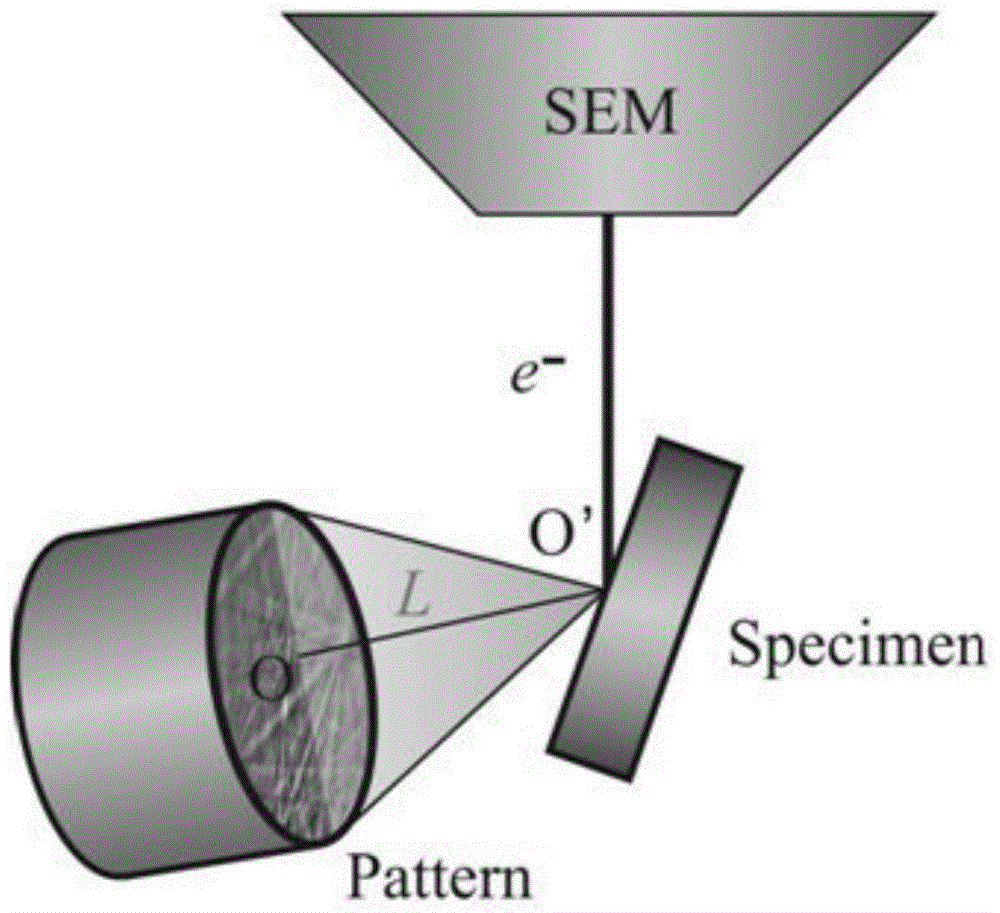
[0038] step 1), figure 1 is a schematic diagram of scanning electron microscope (SEM) and electron backscatter diffraction (EBSD), where point O is the pattern center (PC) of EBSD, point O' is the signal source, and probe distance (DD) is the ratio of L to EBSD image width .
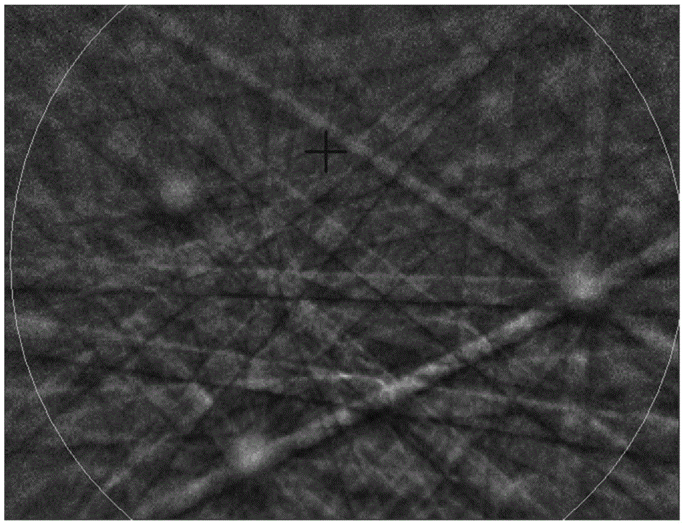
[0039] figure 2 It is the EBSD pattern collected on a certain ore, the image width is 237.1mm, the black cross in the figure is the position of PC, the DD value is 0.6001, the accelerating voltage U=15kV,
[0040] electron beam wavelength λ = 1.5 U ( 1 + 0.9788 × ...
PUM
 Abstract
Description
Claims
Application Information


