
Light-emitting device with dual functions of lighting and communication

A light-emitting device, dual-function technology, applied in the direction of semiconductor devices, electrical components, circuits, etc., can solve the problems of the driving and control circuit technology is far from mature, the luminous capacity of the lighting function is limited, and the international standard has not been formed. Smooth distribution, better effect, reduced area and volume effects

Active Publication Date: 2018-10-26
SOUTH CHINA NORMAL UNIVERSITY
View PDF5 Cites 0 Cited by
  • Summary
  • Abstract
  • Description
  • Claims
  • Application Information

AI Technical Summary

Problems solved by technology

[0002] Lighting-level light-emitting diodes have been available for more than ten years, and the technology of applying light-emitting devices to the communication field has also been studied. However, the promotion and application of this technology are restricted by the corresponding frequency of ordinary LED devices, and the corresponding driving and control circuits The technology is far from mature and has not formed an international standard
Light-emitting devices for communication and applications are still in their infancy, and their lighting functions are also limited due to their light-emitting capabilities.

Method used


Image

  • Light-emitting device with dual functions of lighting and communication
  • Light-emitting device with dual functions of lighting and communication
  • Light-emitting device with dual functions of lighting and communication

Examples


Embodiment

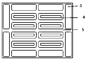
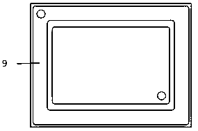
[0019] like figure 1 , figure 2 and image 3 As shown, a light-emitting device with dual functions of illumination and communication includes a substrate layer 1, a buffer layer 10, an n-type layer for generating electrons, a quantum well layer 12 for electron-hole recombination, a p-type layer for generating holes, and A transparent electrode layer 14 , a plurality of communication-type light-emitting chip chips 3 and a plurality of lighting-type chip chips 4 forming a ring structure are deposited on the substrate layer 1 .

[0020] During operation, the n-type layer that generates electrons provides electrons, the p-type layer that generates holes provides charges, and electrons and holes recombine in the quantum well layer 12 where electrons and holes recombine and emit light. The use of ring-shaped chip core particles makes the electron-hole recombination uniform in the quantum well layer 12 of electron-hole recombination, achieving a high recombination rate, so as to a...


PUM


Abstract

The invention discloses a luminescent device with illumination and communication double functions. The luminescent device sequentially comprises a substrate layer, a buffer layer, an n-type layer, a quantum well layer, a p-type layer and a transparent electrode layer, wherein the n-type layer is used for generating electrons; the quantum well layer is compounded with electron holes; the p-type layer is used for generating holes; and a plurality of communication luminous chip core particles for forming a circular structure and a plurality of illumination chip core particles are deposited on the substrate layer. By the chip core particles in the circular structure, the electron holes of the quantum well layer compounded with the electron holes are evenly compounded to reach high compound rate, therefore, the technical effects of high speed and wide band of the device are reached; meanwhile, the chip core particles form the circular structure; the area and the volume of the chip core particles are reduced; and the response rate of the device is improved.

Description

technical field [0001] The invention relates to the field of optoelectronic devices, in particular to a light emitting device with dual functions of illumination and communication. Background technique [0002] Lighting-level light-emitting diodes have been available for more than ten years, and the technology of applying light-emitting devices to the communication field has also been studied. However, the promotion and application of this technology are restricted by the corresponding frequency of ordinary LED devices, and the corresponding driving and control circuits The technology is far from mature, and no international standard has been formed. Light-emitting devices for communication and applications are still in their infancy, and their lighting functions are also limited due to their light-emitting capabilities. White LEDs have the characteristics of short response time and high-speed modulation, and can be used in the fields of visible light lighting and communica...

Claims


Application Information

Patent Timeline
Patent Type & Authority Patents(China)
IPC IPC(8): H01L33/00H01L33/06H01L33/48
CPCH01L33/00H01L33/06H01L33/48
Inventor 孙慧卿黄鸿勇张柱定张诚李旭娜孙浩范宣聪黄涌郭志友
Owner SOUTH CHINA NORMAL UNIVERSITY
Learn More