A kind of pad window opening method and pcb board

A technology for PCB boards and pads, which is applied to the pad windowing method and the field of PCB boards, can solve the problems of PCB board product performance degradation, pin distortion, biased micro-electronic devices, etc., so as to improve the welding quality and prevent spillage. , Improve the effect of arrangement uniformity

Active Publication Date: 2018-08-07
ZHUHAI FOUNDER TECH HI DENSITY ELECTRONICS +1
View PDF3 Cites 0 Cited by
  • Summary
  • Abstract
  • Description
  • Claims
  • Application Information

AI Technical Summary

Problems solved by technology

[0008] Therefore, the object of the present invention is to overcome the problem that the pins are prone to twisting and / or distortion when using solder paste to weld the pads and pins after removing the insulating ink covering the pads in the prior art. Or pull the microelectronic device, so that the technical defect of the PCB board product performance is seriously reduced, so as to provide a method that can completely remove the insulating ink covering the pad, and enable the pad to be welded with the pin through solder paste. Pad window opening method to slow down the twisting and deformation of pins and improve the uniformity of pin arrangement

Method used


Image

  • A kind of pad window opening method and pcb board
  • A kind of pad window opening method and pcb board

Examples


Embodiment 1

[0034]This embodiment provides a pad window opening method, including the following steps:

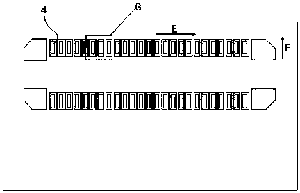
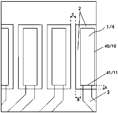
[0035] 1) Set a shading area on the film, such as Figure 1-2 As shown, the shading area includes a pad shading area 1 for covering the pad 4 and a buffer zone 2 surrounding the pad shading area 1; the pad 4 has a connection edge 41 connected to the line 3 and not The non-connecting side 40 connected to the line 3, the pad light-shielding area 1 has a light-shielding area connecting side 11 corresponding to the connecting side 41 and a light-shielding area non-wiring side 10 corresponding to the non-wiring side 40, and is set to The width A of the buffer zone where the connecting edge 11 of the shading area is the inner edge is 0.6mil, and the width B of the buffer zone with the non-connecting edge 10 of the shading area being the inner edge is set to be 2.35mil; The distance between them is 3mil;

[0036] 2) Adjust the alignment accuracy of the alignment exposure machine to less tha...

Embodiment 2

[0043] This embodiment provides a pad window opening method, which is a modification based on Embodiment 1, and specifically includes the following steps:

[0044] 1) Read the film data information containing the buffer zone 2 and the width of the buffer zone 2 is 2.4mil into the Genesis / Incam design software system. The wiring edge 10 is the buffer zone of the inner edge. In this step, adjust the width A of the buffer zone with the light-shielding wiring edge 11 as the inner edge to be 0.6mil;

[0045] 2) Adjust the alignment accuracy of the alignment exposure machine to be less than 0.6mil, and then use the alignment exposure machine to align the film with the PCB board provided with the pad 4, so that the pad shading area 1 is aligned with the pad 4 After the pads 4 are aligned, the PCB board is exposed and developed, so that the pads 4 are completely exposed, and the windowing of the pads is completed.

[0046] The pad window opening method of this embodiment is based on ...

Embodiment 3

[0052] This embodiment provides a PCB board, and the pads of the PCB board in this embodiment are prepared by using the pad window opening method in Embodiment 1 or Embodiment 2.

[0053] Since the pads on the PCB of this embodiment are prepared by the above-mentioned pad window opening method, the PCB board of the present invention has all the advantages of using the above pad window opening method.


PUM


Abstract

The invention provides a bonding pad windowing method and a printed circuit board (PCB). The windowing method comprises the following steps of: arranging a shading region on a film roll, wherein the shading region comprises a bonding pad shading region for covering a bonding pad and a buffer region encircling the bonding pad shading region, the bonding pad is provided with a wiring edge and a non-wiring edge, the bonding pad shading region is provided with a shading region wiring edge corresponding to the wiring edge and a shading region non-wiring edge corresponding to the non-wiring edge, and the width of the buffer region taking the shading region wiring edge as an inner edge is smaller than the width of the buffer region taking the shading region non-wiring edge as an inner edge; and aligning the film roll to the PCB designed with the bonding pad, exposing and developing the PCB to make the bonding pad completely exposed, and completing the windowing of the bonding pad. According to the bonding pad windowing method provided by the invention, the circuit length exposed after exposure and development is short, and the influence of a circuit on the center of the bonding pad is low; when the bonding pad and a pin are welded through a tin paste, the condition that a miniature electronic device is pulled and deviated by the pin is greatly improved; and moreover, the condition that the pin is twisted and deformed is also relieved.

Description

technical field [0001] The invention relates to a pad window opening method and a PCB board, belonging to the technical field of pad window opening methods for PCB boards. Background technique [0002] In order to expand the functions of PCB products, it is sometimes necessary to add microelectronic devices that are electrically connected to the PCB on the PCB. The existing way to achieve electrical conduction between the microelectronic devices and the PCB is generally to set pins on the microelectronic devices. Pads corresponding to the pins are provided on the PCB, and electrical conduction between the microelectronic device and the PCB is realized by welding the pins to the pads. In the production process of PCB boards, the pads set on the PCB board are often covered by insulating ink (that is, often called green oil or green paint). In order to re-expose the pads covered by insulating ink, it is necessary to cover them The insulating ink on the pad is removed. This pro...

Claims


Application Information

Patent Timeline
Patent Type & Authority Patents(China)
IPC IPC(8): H05K3/02H05K3/34
CPCH05K3/027H05K3/3452H05K2203/0557
Inventor 葛春朱兴华
Owner ZHUHAI FOUNDER TECH HI DENSITY ELECTRONICS
Why Eureka
Try Eureka