

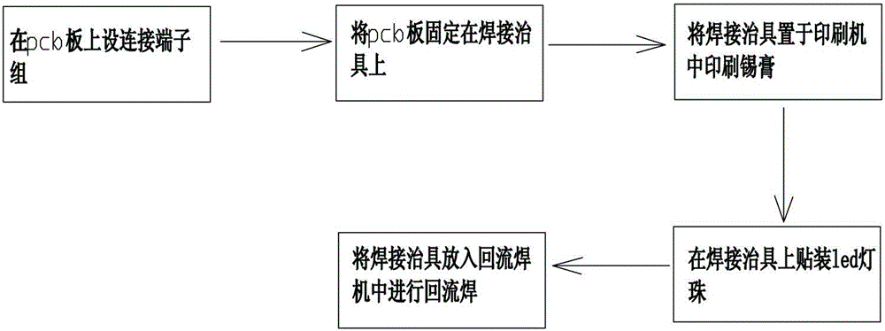
Method for arranging LED lamp beads on side face of PCB in surface-mounting manner
A technology of LED lamp beads and PCB boards, which is applied to lighting devices, components of lighting devices, printed circuits connected with non-printed electrical components, etc., can solve problems such as affecting lighting, low production efficiency, and affecting appearance, and achieve Speed up the placement accuracy, speed up the placement, and improve the stability of the effect
- Summary
- Abstract
- Description
- Claims
- Application Information
AI Technical Summary
Problems solved by technology
Method used
Image

Examples
Embodiment Construction
[0028] In the description of the present invention, it should be understood that the orientation or positional relationship indicated by the terms "center", "upper", "lower", "front", "rear", "left", "right" etc. are based on The orientation or positional relationship shown in the drawings is only for the convenience of describing the present invention and simplifying the description, and does not indicate or imply that the referred device or element must have a specific orientation, be constructed and operated in a specific orientation, and therefore cannot be understood as Limitations on the Invention. In addition, the terms "first" and "second" are used for descriptive purposes only, and should not be understood as indicating or implying relative importance.
[0029] In the description of the present invention, it should be noted that unless otherwise specified and limited, the terms "installation", "connection" and "connection" should be understood in a broad sense, for ex...
PUM
 Abstract
Description
Claims
Application Information