Display substrate and manufacturing method thereof and display device

A technology for displaying substrates and manufacturing methods, applied in semiconductor/solid-state device manufacturing, electrical components, electrical solid-state devices, etc., can solve the problems of poor adsorption and detachment between flat layers and transparent conductive layers, so as to ensure performance and increase adhesion , Improve the effect of product quality

Inactive Publication Date: 2015-12-30
BOE TECH GRP CO LTD
View PDF3 Cites 5 Cited by
  • Summary
  • Abstract
  • Description
  • Claims
  • Application Information

AI Technical Summary

Problems solved by technology

[0004] The present invention provides a display substrate and a manufacturing method thereof, which are used to solve the problem that the f

Method used


Image

  • Display substrate and manufacturing method thereof and display device
  • Display substrate and manufacturing method thereof and display device

Examples


Embodiment Construction

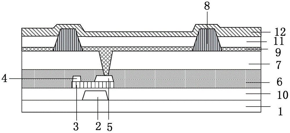
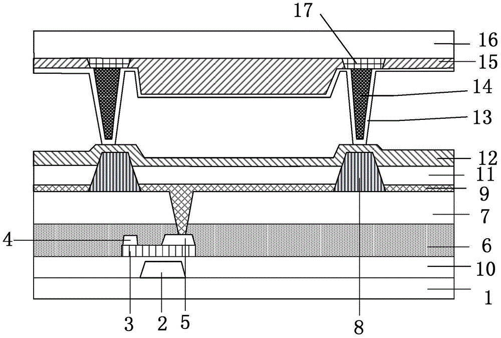
[0017] The present invention provides a display substrate, including a flat layer for providing a platform surface, the material of the flat layer includes organic silicon, because organic silicon has both the properties of organic materials and inorganic materials, so that the flat layer and the organic material thin film and The inorganic material film has good adhesion, prevents the flat layer from peeling off from adjacent films, ensures the performance of the display substrate, and improves product quality.

[0018] Among them, organosilicon is an organosilicon compound, which refers to a compound containing Si-C bonds, and at least one organic group is directly connected to a silicon atom. Compounds in which atoms are linked are also referred to as organosilicon compounds. Among them, the polysiloxane composed of silicon-oxygen bond (-Si-0-Si-) as the skeleton is the most numerous, the deepest researched and the most widely used class of organosilicon compounds, accounti...


PUM


Abstract

The invention relates to the technical field of display, and discloses a display substrate and a manufacturing method thereof and a display device. The flat layer of the display substrate is made of organosilicon material. The organosilicon has performance of both organic material and inorganic material so that adhesiveness of the flat layer and an organic material thin-film and an inorganic material thin-film can be increased, the flat layer can be prevented from being separated from the interface of the adjacent thin-film, performance of the display substrate can be guaranteed and product quality can be enhanced.

Description

technical field [0001] The invention relates to the field of display technology, in particular to a display substrate, a manufacturing method thereof, and a display device. Background technique [0002] At present, in an active matrix organic light emitting diode (ActiveMatrix / OrganicLightEmittingDiode, abbreviated as AMOLED) display device, the structure of its array substrate can be found in figure 1 1 is the base substrate of the array substrate; 2 is the gate electrode; 3 is the active layer; 4 is the source electrode; 5 is the drain electrode; 6 is the inorganic insulating layer; 7 is the flat layer; 8 is the pixel definition layer (PixelDefineLayer, PDL); 9 is an anode, including transparent conductive material and metal silver; 10 is a gate insulating layer; 11 is an organic light-emitting layer; 12 is a cathode. [0003] In the prior art, the flat layer 7 is usually made of organic material, such as organic resin, which has simple processing technology and can provi...

Claims


Application Information

Patent Timeline
IPC IPC(8): H01L27/32H01L21/02
CPCH10K59/124
Inventor 胡月刘则
Owner BOE TECH GRP CO LTD
Why Eureka
Try Eureka